APPLICATIONS
l 400GAUI-8
l Other 400G optical links
Compliance
l QSFP-DD MSA.
l RoHS
Ordering information
|
Package |
Product part NO. |
Distance |
Temperature Range |
|
QSFP-DD |
ESWSAA31-M01C |
1-metercable |
Commercial: 0~70℃ |
|
QSFP-DD |
ESWSAA31-M03C |
3-metercable |
Commercial: 0~70℃ |
|
QSFP-DD |
ESWSAA31-M05C |
5-metercable |
Commercial: 0~70℃ |
|
QSFP-DD |
ESWSAA31-M07C |
7-metercable |
Commercial: 0~70℃ |
|
QSFP-DD |
ESWSAA31-M10C |
10-metercable |
Commercial: 0~70℃ |
|
QSFP-DD |
ESWSAA31-M15C |
15-metercable |
Commercial: 0~70℃ |
|
QSFP-DD |
ESWSAA31-M20C |
20-metercable |
Commercial: 0~70℃ |
|
QSFP-DD |
ESWSAA31-M30C |
30-metercable |
Commercial: 0~70℃ |
|
*For availability of additional cable lengths, please contact Esion.
|
|||
I. Pin Diagram

II. Pin Descriptions
|
Pad |
Symbol |
Description |
Ref. |
|
1 |
GND |
Ground |
|
|
2 |
Tx2n |
Transmitter Inverted Data Input |
|
|
3 |
Tx2p |
Transmitter Non-Inverted Data Input |
|
|
4 |
GND |
Ground |
|
|
5 |
Tx4n |
Transmitter Inverted Data Input |
|
|
6 |
Tx4p |
Transmitter Non-Inverted Data Input |
|
|
7 |
GND |
Ground |
|
|
8 |
ModSelL |
Module Select |
|
|
9 |
ResetL |
Module Reset |
|
|
10 |
VccRx |
+3.3V Power Supply Receiver |
|
|
Pad |
Symbol |
Description |
Ref. |
|
11 |
SCL |
2-wire serial interface clock |
|
|
12 |
SDA |
2-wire serial interface data |
|
|
13 |
GND |
Ground |
|
|
14 |
Rx3p |
Receiver Non-Inverted Data Output |
|
|
15 |
Rx3n |
Receiver Inverted Data Output |
|
|
16 |
GND |
Ground |
|
|
17 |
Rx1p |
Receiver Non-Inverted Data Output |
|
|
18 |
Rx1n |
Receiver Inverted Data Output |
|
|
19 |
GND |
Ground |
|
|
20 |
GND |
Ground |
|
|
21 |
Rx2n |
Receiver Inverted Data Output |
|
|
22 |
Rx2p |
Receiver Non-Inverted Data Output |
|
|
23 |
GND |
Ground |
|
|
24 |
Rx4n |
Receiver Inverted Data Output |
|
|
25 |
Rx4p |
Receiver Non-Inverted Data Output |
|
|
26 |
GND |
Ground |
|
|
27 |
ModPrsL |
Module Present |
|
|
28 |
IntL |
Interrupt |
|
|
29 |
VccTx |
+3.3V Power supply transmitter |
|
|
30 |
Vcc1 |
+3.3V Power supply |
|
|
31 |
LPMode |
Low Power mode; |
|
|
32 |
GND |
Ground |
|
|
33 |
Tx3p |
Transmitter Non-Inverted Data Input |
|
|
34 |
Tx3n |
Transmitter Inverted Data Input |
|
|
35 |
GND |
Ground |
|
|
36 |
Tx1p |
Transmitter Non-Inverted Data Input |
|
|
37 |
Tx1n |
Transmitter Inverted Data Input |
|
|
38 |
GND |
Ground |
|
|
39 |
GND |
Ground |
|
|
40 |
Tx6n |
Transmitter Inverted Data Input |
|
|
41 |
Tx6p |
Transmitter Non-Inverted Data Input |
|
|
42 |
GND |
Ground |
|
|
43 |
Tx8n |
Transmitter Inverted Data Input |
|
|
44 |
Tx8p |
Transmitter Non-Inverted Data Input |
|
|
45 |
GND |
Ground |
|
|
46 |
Reserved |
For future use |
|
|
47 |
VS1 |
Module Vendor Specific 1 |
|
|
48 |
VccRx1 |
3.3V Power Supply |
|
|
Pad |
Symbol |
Description |
Ref. |
|
49 |
VS2 |
Module Vendor Specific 2 |
|
|
50 |
VS3 |
Module Vendor Specific 3 |
|
|
51 |
GND |
Ground |
|
|
52 |
Rx7p |
Receiver Non-Inverted Data Output |
|
|
53 |
Rx7n |
Receiver Inverted Data Output |
|
|
54 |
GND |
Ground |
|
|
55 |
Rx5p |
Receiver Non-Inverted Data Output |
|
|
56 |
Rx5n |
Receiver Inverted Data Output |
|
|
57 |
GND |
Ground |
|
|
58 |
GND |
Ground |
|
|
59 |
Rx6n |
Receiver Inverted Data Output |
|
|
60 |
Rx6p |
Receiver Non-Inverted Data Output |
|
|
61 |
GND |
Ground |
|
|
62 |
Rx8n |
Receiver Inverted Data Output |
|
|
63 |
Rx8p |
Receiver Non-Inverted Data Output |
|
|
64 |
GND |
Ground |
|
|
65 |
NC |
No Connect |
|
|
66 |
Reserved |
For future use |
|
|
67 |
VccTx1 |
3.3V Power Supply |
|
|
68 |
Vcc2 |
3.3V Power Supply |
|
|
69 |
Reserved |
For future use |
|
|
70 |
GND |
Ground |
|
|
71 |
Tx7p |
Transmitter Non-Inverted Data Input |
|
|
72 |
Tx7n |
Transmitter Inverted Data Input |
|
|
73 |
GND |
Ground |
|
|
74 |
Tx5p |
Transmitter Non-Inverted Data Input |
|
|
75 |
Tx5n |
Transmitter Inverted Data Input |
|
|
76 |
GND |
Ground |
|
III. Absolute Maximum Ratings
|
Parameter |
Symbol |
Min. |
Typ. |
Max. |
Unit |
Ref. |
|
Storage Temperature |
TS |
-40 |
|
85 |
ºC |
|
|
Storage Ambient Humidity |
HA |
0 |
|
85 |
% |
|
|
Maximum Supply Voltage |
VCC |
-0.5 |
|
3.6 |
V |
|
|
Lead Soldering Temperature/Time |
TSOLD |
|
|
260/10 |
ºC/sec |
1 |
|
Lead Soldering Temperature/Time |
TSOLD |
|
|
360/10 |
ºC/sec |
2 |
Note:
1.Suitable for wave soldering.
2. Only for soldering by iron.
IV. Recommended Operating Conditions
|
Data Rate Spcifications |
Symbol |
Min. |
Typ. |
Max. |
Unit |
Ref. |
|
Supply Voltage |
Vcc |
3.13 |
3.3 |
3.47 |
V |
|
|
Baud Rate(per channel ) PAM4 |
BR |
|
26.5625 |
|
GBd |
1 |
|
Operating Case Temperature |
Tc |
0 |
|
70 |
℃ |
|
|
Link distance on OM4 MMF |
d |
|
|
100 |
meters |
|
Notes:
1. Per channel,PAM4.
V. Electrical Interface Characteristics
|
Parameter |
Symbol |
Min. |
Typ. |
Max. |
Unit |
Ref. |
|
Supply Voltage |
VCC1, VCCTX, VCCRX |
3.15 |
|
3.45 |
V |
|
|
Power Dissipation |
Pd |
|
|
10 |
W |
|
|
Transmitter(per Lane) |
||||||
|
Input different impedance |
Rin |
90 |
100 |
110 |
Ω |
|
|
Single ended input voltage tolerance |
VinT |
-0.3 |
|
4.0 |
V |
|
|
Differential Input Voltage Amplitude |
Vin,pp |
|
|
900 |
mV |
|
|
Receiver (per Lane) |
||||||
|
Error Bit Rate |
BER |
|
|
2.4E-4 |
|
|
|
Output different impedance |
Rout |
90 |
100 |
110 |
Ω |
|
|
Single-ended output voltage |
VoutR |
-0.3 |
|
4.0 |
V |
|
|
Differential Output Voltage Amplitude |
Vout,pp |
|
|
900 |
mV |
|
VI. Digital Diagnostic Functions
Compatible with QSFP-DD CMIS rev 4.0.
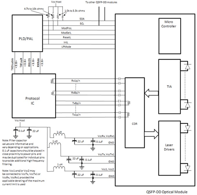
VII. Recommended Interface Circuit

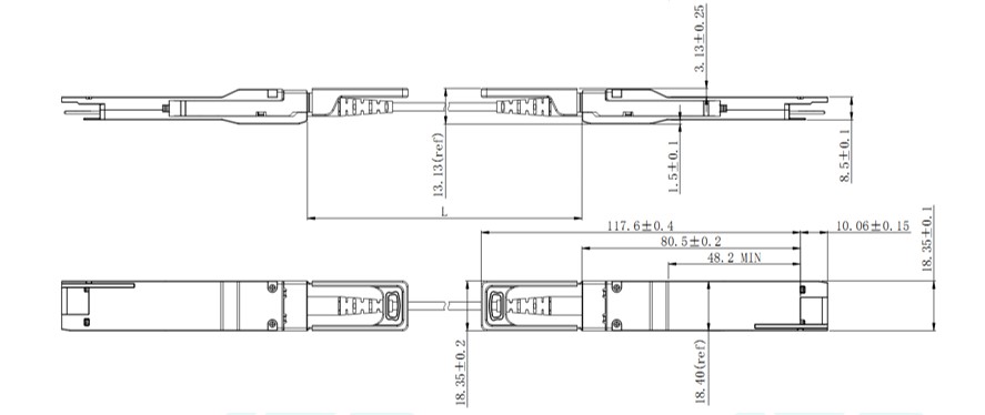
VIII.Mechanical Specifications (Unit: mm)

|
Cable Length(Unit: m) |
Tolerant(Unit: cm) |
|
<1.0 |
+10/-0 |
|
1.0~4.5 |
+20/-0 |
|
5.0~14.5 |
+40/-0 |
|
≥15.0 |
+3%/-0 |
Want to know about this product?
If you are interested in our products and want to know more details,please leave a message here,we will reply you as soon as we can.