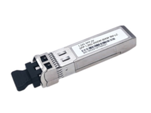
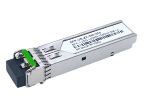
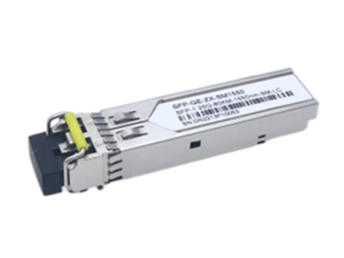
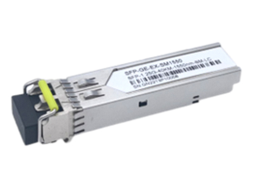
Applications
l 1000BASE-EX Ethernet
l 1.06Gb/s Fibre Channel
Compliance
l SFP MSA
l SFF-8472
l IEEE802.3z
l ROHS
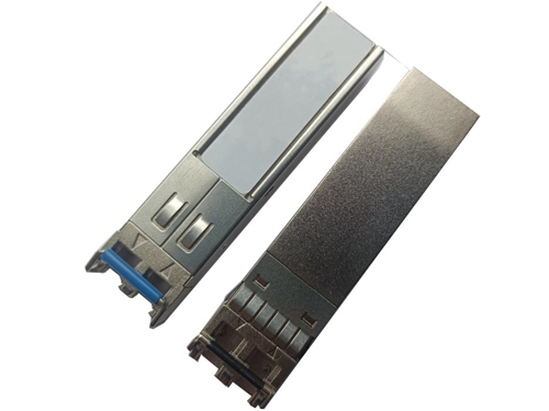
Ordering information
|
Part No. |
Bit Rate (Gbps) |
Laser (nm) |
Distance(km) |
Fiber Type |
DDMI |
Connector |
Temp |
|
ESGCLB31-K40C |
1.25 |
1310 |
40 |
SMF |
YES |
LC |
0℃~70℃ |
|
ESGCLB31-K40E |
1.25 |
1310 |
40 |
SMF |
YES |
LC |
-20℃~85℃ |
|
ESGCLB31-K40I |
1.25 |
1310 |
40 |
SMF |
YES |
LC |
-40℃~85℃ |
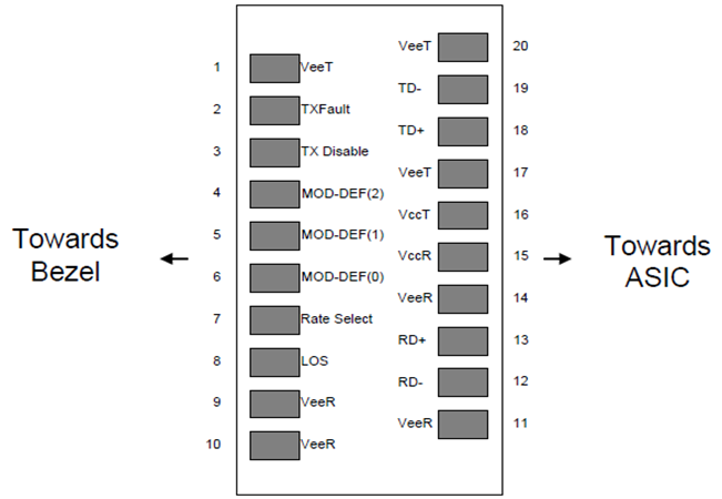
Pinout of Connector Block on Host Board
Pin Descriptions
|
Pin |
Symbol |
Name/Description |
Ref. |
|
1 |
VEET |
Transmitter Ground (Common with Receiver Ground) |
1 |
|
2 |
TFAULT |
Transmitter Fault. |
2 |
|
3 |
TDIS |
Transmitter Disable. Laser output disabled on high or open. |
3 |
|
4 |
MOD_DEF(2) |
Module Definition 2. Data line for Serial ID. |
4 |
|
5 |
MOD_DEF(1) |
Module Definition 1. Clock line for Serial ID. |
4 |
|
6 |
MOD_DEF(0) |
Module Definition 0. Grounded within the module. |
4 |
|
7 |
Rate Select |
No connection required |
|
|
8 |
LOS |
Loss of Signal indication. Logic “0” indicates normal operation. |
5 |
|
9 |
VEER |
Receiver Ground (Common with Transmitter Ground) |
|
|
10 |
VEER |
Receiver Ground (Common with Transmitter Ground) |
1 |
|
11 |
VEER |
Receiver Ground (Common with Transmitter Ground) |
1 |
|
12 |
RD- |
Receiver Inverted DATA out (CML). AC Coupled |
|
|
13 |
RD+ |
Receiver Non-inverted DATA out (CML). AC Coupled |
|
|
14 |
VEER |
Receiver Ground (Common with Transmitter Ground) |
1 |
|
15 |
VCCR |
Receiver Power Supply |
|
|
16 |
VCCT |
Transmitter Power Supply |
|
|
17 |
VEET |
Transmitter Ground (Common with Receiver Ground) |
1 |
|
18 |
TD+ |
Transmitter Non-Inverted DATA in. AC Coupled. |
|
|
19 |
TD- |
Transmitter Inverted DATA in. AC Coupled. |
|
|
20 |
VEET |
Transmitter Ground (Common with Receiver Ground) |
1 |
Notes:
1. Circuit ground is internally isolated from chassis ground.
2. TFAULT is an open collector/drain output, which is pulled up with a 4.7kΩ – 10kΩ resistor on the host board, but is grounded inside the SFP cable plug.
3. Laser output disabled on TDIS >2.0V or open, enabled on TDIS <0.8V.
4. Mod-Def 0,1,2. These are the module definition pins. They should be pulled up with a 4.7K – 10KΩ resistor on the host board. The pull-up voltage shall be VccT or VccR
Mod-Def 0 is grounded by the module to indicate that the module is present
Mod-Def 1 is the clock line of two wire serial interface for serial ID
Mod-Def 2 is the data line of two wire serial interface for serial ID
5. LOS is open collector output. Should be pulled up with 4.7kΩ – 10kΩ on host board to a voltage between 2.0V and 3.6V. Logic 0 indicates normal operation; logic 1 indicates loss of signal.
Absolute Maximum Ratings
|
Parameter |
Symbol |
Min |
Type |
Max |
Unit |
Ref. |
|
Maximum Supply Voltage |
Vcc |
-0.5 |
|
3.6 |
V |
|
|
Storage Temperature |
TS |
-40 |
|
85 |
℃ |
|
|
Case Operating Temperature |
TOP |
0 |
|
70 |
℃ |
Commercial |
|
-20 |
|
85 |
Extended |
|||
|
-40 |
|
85 |
Industrial |
|||
|
Relative Humidity |
RH |
0 |
|
85 |
% |
1 |
Notes:
1. Non-condensing.
Optical Characteristics (TOP = 0°C to 70°C, VCC = 3.3 ± 5% Volts)
|
Parameter |
Symbol |
Min. |
Typ. |
Max. |
Unit |
Remark |
|
Transmitter |
||||||
|
Center Wavelength |
λc |
1290 |
1310 |
1330 |
nm |
|
|
Spectral Width(-20dB) |
Pm |
|
|
1 |
nm |
|
|
Side-mode Suppression Ratio |
SMSR |
30 |
|
|
dB |
|
|
Average Output Power |
Pavg |
-5 |
|
0 |
dBm |
|
|
Extinction Ratio |
ER |
9 |
|
|
dB |
|
|
Return Loss |
|
12 |
|
|
dB |
|
|
Transmitter OFF Output Power |
POff |
|
|
-30 |
dBm |
|
|
Receiver |
||||||
|
Center Wavelength |
λc |
1260 |
|
1600 |
nm |
|
|
Receiver Sensitivity, Average Power |
|
|
|
-24 |
dBm |
|
|
Receiver Saturation Power |
Psat |
|
|
0 |
dBm |
|
|
Loss of Signal Assert |
PA |
-35 |
|
|
dBm |
|
|
Loss of Signal De-assert |
PD |
|
|
-25 |
dBm |
|
|
LOS Hysteresis |
PD- PA |
0.5 |
|
|
Db |
|
Electrical Characteristics (TOP = 0°C to 70°C, VCC = 3.3 ± 5% Volts)
|
Parameter |
Symbol |
Min |
Type |
Max |
Unit |
Ref. |
|
Supply Voltage |
Vcc |
3.135 |
3.3 |
3.465 |
V |
|
|
Supply Current |
Icc |
|
|
300 |
Ma |
|
|
Transmitter |
||||||
|
Input differential impedance |
Rin |
|
100 |
|
|
1 |
|
Differential data input swing |
Vin, pp |
200 |
|
1000 |
Mv |
|
|
Transmit Disable Voltage |
VD |
2 |
|
VCC |
V |
|
|
Transmit Enable Voltage |
VEN |
Vee |
|
Vee+0.8 |
V |
|
|
Receiver |
||||||
|
Differential data output swing |
Vout, pp |
200 |
|
1000 |
Mv |
2 |
|
LOS Fault |
VLOS_fault |
2 |
|
Vcc |
V |
3 |
|
LOS Normal |
VLOS_norm |
Vee |
|
Vee+0.8 |
V |
3 |
|
Power Supply Noise Tolerance |
VCCT/VCCR |
Per SFP MSA |
mVpp |
|
||
Notes:
1. Connected directly to TX data input pins.AC coupling from pins into laser driver IC.
2. Into 100Ω differential termination.
3. Loss Of Signal is LVTTL. Logic 0 indicates normal operation; logic 1 indicates no signal detected.
Digital Diagnostic Memory Map
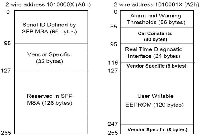
Digital Diagnostic Monitoring Information
|
Parameter |
Unit |
Accuracy |
|
Case Temperature |
℃ |
±3 |
|
Supply Voltage |
V |
±3% |
|
Tx Bias Current |
Ma |
±10% |
|
Tx Optical Power |
Db |
±3 |
|
Rx Optical Power |
Db |
±3 |
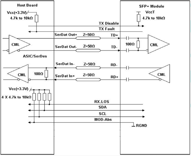
Recommended Interface Circuit
Mechanical Dimensions
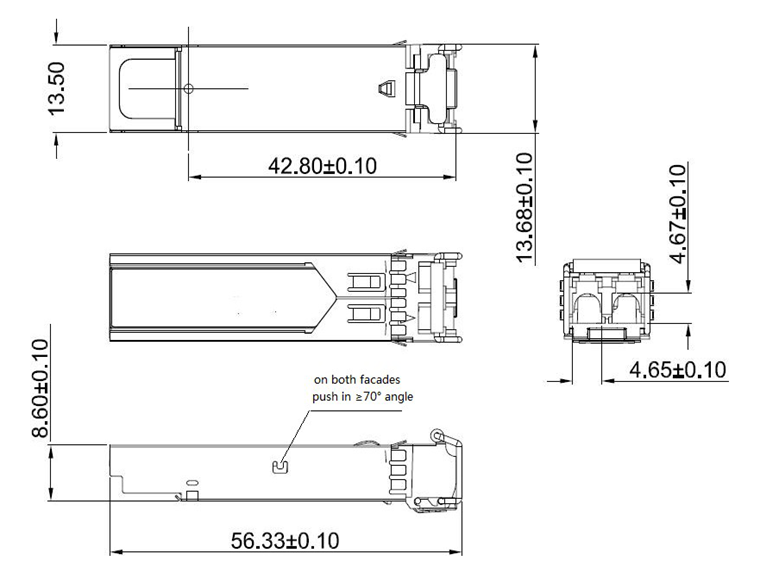
SFP wire mechanical drawing (Unit: mm)
Want to know about this product?
If you are interested in our products and want to know more details,please leave a message here,we will reply you as soon as we can.
 LPGCLM85-S55C(I)
 LPGCLF31-K40C(I)
 LPGCLF31-K10(20)C(I)
 LPGCLDxx-K80C
 LPGCLB55-Z16C(I)
 LPGCLB55-Z15C(I)
 LPGCLB55-Z10C(I)
 LPGCLB55-K80C(I)
 LPGCLB55-K60C(I)
 LPGCLB55-K40C(I)

Address : East of 2F, Tianmen Optical Valley Science Park,Qiaoxiang Economic development area,Tianmen, Hubei Province.
Tel : 15012662571
Email : chris.peng@talptech.com
Skype : 15012662571