APPLICATIONS
l 200GBASE-FR4 Ethernet
l Switch & Router Connections
l Data Centers
Other 200G Interconnect RequirementsCompliance
l IEEE802.3cd
l CMIS Rev4.0
l OIF-CEI-04.0 56G-VSR-PSM4
l IEEE802.3bs Annex120E
l SFF-8024 Rev.4.6
l SFF-8679 Rev1.8
l SFF-8665 Rev1.9
Ordering information
|
Part NO. |
Bit Rate (Gbps) |
Laser (nm) |
Distance (km) |
Media |
DDMI |
Detector |
Temp(℃) |
|
ESCRLB31-K02C |
212.5 |
1264.5~1277.5 1284.5~1297.5 1304.5~1317.5 1324.5~1337.5 |
2 |
SMF |
YES |
PIN |
0~70 |
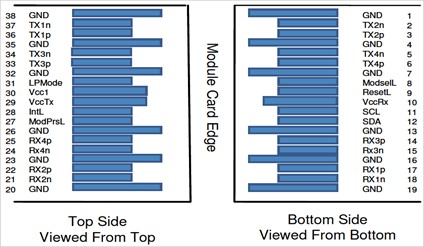
I. Pin Diagram
 Electrical Pin-out Details
II. Pin Descriptions
|
Pin |
Symbol |
Name/Description |
Ref. |
|
1 |
GND |
Ground |
1 |
|
2 |
Tx2n |
Transmitter Inverted Data Input |
|
|
3 |
Tx2p |
Transmitter Non-Inverted Data Input |
|
|
4 |
GND |
Ground |
1 |
|
5 |
Tx4n |
Transmitter Inverted Data Input |
|
|
6 |
Tx4p |
Transmitter Non-Inverted Data Input |
|
|
7 |
GND |
Ground |
1 |
|
8 |
ModSe1L |
Module Select |
|
|
9 |
ResetL |
Module Reset |
|
|
10 |
Vcc Rx |
+3.3V Power supply receiver |
|
|
11 |
SCL |
2-wire serial interface clock |
|
|
12 |
SDA |
2-wire serial interface data |
|
|
13 |
GND |
Ground |
1 |
|
14 |
Rx3p |
Receiver Non-Inverted Data Output |
|
|
15 |
Rx3n |
Receiver Inverted Data Output |
|
|
16 |
GND |
Ground |
1 |
|
17 |
Rx1p |
Receiver Non-Inverted Data Output |
|
|
18 |
Rx1n |
Receiver Inverted Data Output |
|
|
19 |
GND |
Ground |
1 |
|
20 |
GND |
Ground |
1 |
|
21 |
Rx2n |
Receiver Inverted Data Output |
|
|
22 |
Rx2p |
Receiver Non-Inverted Data Output |
|
|
23 |
GND |
Ground |
1 |
|
24 |
Rx4n |
Receiver Inverted Data Output |
|
|
25 |
Rx4p |
Receiver Non-Inverted Data Output |
|
|
26 |
GND |
Ground |
1 |
|
27 |
ModPrSL |
Module Present |
|
|
28 |
IntL |
Interrupt |
|
|
29 |
Vcc Tx |
+3.3V Power supply transmitter |
|
|
30 |
Vcc1 |
+3.3V Power Supply |
|
|
31 |
LPMode |
Low Power Mode |
|
|
32 |
GND |
Ground |
1 |
|
33 |
Tx3p |
Transmitter Non-Inverted Data Input |
|
|
34 |
Tx3n |
Transmitter Inverted Data Input |
|
|
35 |
GND |
Ground |
1 |
|
36 |
Tx1p |
Transmitter Non-Inverted Data Input |
|
|
37 |
Tx1n |
Transmitter Inverted Data Input |
|
|
38 |
GND |
Ground |
1 |
Note:
QSFP56 uses common ground (GND) for all signals and supply (power). All the common within the QSFP56 module and all module voltages are referenced to this potential unless otherwise noted. Connected theses directly to the host board signal common ground plane.
VccRx, VccRx1, Vcc1, Vcc2, VccTx, and VccTx1 shall be applied concurrently. Requirements defined for the host side of the Host Card Edge Connector are listed in Table 4. VccRx, VccRx1, Vcc1, Vcc2, VccTx, and VccTx1 may be internally connected within the module in any combination. The connector Vcc pins are each rated for a maximum current of 1000mA.
All Vendor Specific, Reserved and No Connect pins may be terminated with 50 ohms to ground on the host. Pad 65 (No Connect) shall be left unconnected within the module. Vendor Specific and Reserved pads shall have an impedance to GND that is greater than 10 kOhms and less than 100pF
III. Absolute Maximum Ratings
|
Parameter |
Symbol |
Min. |
Typ. |
Max. |
Unit |
Ref. |
|
Storage Temperature Range |
TS |
-40 |
|
85 |
ºC |
|
|
Relative Humidity |
HA |
5 |
|
85 |
% |
|
|
Power Supply Voltage |
VCC |
-0.5 |
|
4.0 |
V |
|
IV. Recommended Operating Conditions
|
Data Rate Spcifications |
Symbol |
Min. |
Typ. |
Max. |
Unit |
Ref. |
|
Supply Voltage |
Vcc |
3.135 |
3.3 |
3.465 |
V |
|
|
Baud Rate(per channel ) |
BR |
|
26.5625 |
|
GBd |
|
|
Operating Case Temperature Range |
Tc |
0 |
|
70 |
℃ |
|
V. Optical Characteristics
|
Parameter Unit |
Symbol |
Min. |
Min. |
Typ. |
Max. |
Ref. |
|
Transmitter(per lane) |
||||||
|
Signaling Speed per Lane |
|
GBd |
|
26.5625 |
|
|
|
Modulation format |
|
|
|
PAM4 |
|
|
|
Center wavelength |
WL |
nm |
1264.5 |
1271 |
1277.5 |
|
|
nm |
1284.5 |
1291 |
1297.5 |
|
||
|
nm |
1304.5 |
1311 |
1317.5 |
|
||
|
nm |
1324.5 |
1331 |
1337.5 |
|
||
|
Side-mode suppression Ratio |
SMSR |
dB |
30 |
|
|
|
|
Average Launch Power per Lane |
TXPx |
dBm |
-4.2 |
|
4.7 |
|
|
Tx OMA per lane |
TxOMA |
dBm |
-1.2 |
|
4.5 |
|
|
Optical Extinction Ratio |
ER |
dB |
3.5 |
|
|
|
|
Transmitter and dispersion eye closure for PAM4 per Lane |
TDECQ |
dB |
|
|
3.3 |
|
|
Optical Return Loss Tolerance |
ORL |
dB |
|
|
16.5 |
|
|
Relative Intensity Noise |
RIN |
Db/Hz |
|
|
-132 |
|
|
Receiver(per lane) |
||||||
|
Signaling Speed per Lane |
|
GBd |
|
26.5625 |
|
|
|
Center wavelength |
WL |
nm |
1264.5 |
1271 |
1277.5 |
|
|
nm |
1284.5 |
1291 |
1297.5 |
|
||
|
nm |
1304.5 |
1311 |
1317.5 |
|
||
|
nm |
1324.5 |
1331 |
1337.5 |
|
||
|
Damage Threshold |
DT |
dBm |
5.7 |
|
|
|
|
Average receive Power per Lane |
RXPx |
dBm |
-8.2 |
|
4.7 |
|
|
Receiver reflectance |
Rfl |
dB |
|
|
-26 |
|
|
Receiver sensitivity (OMA outer ), (each lane,max) |
|
dBm |
|
|
-6 |
|
|
Stressed receiver sensitivity (OMAouter) ,each lane |
|
dBm |
|
|
-3.6 |
|
VI. Electrical Interface Characteristics
|
Parameter |
Symbol |
Unit |
Min. |
Typ. |
Max. |
Ref. |
|
Supply Voltage |
VCC |
V |
3.135 |
3.3 |
3.465 |
|
|
Power Consumption |
Pc |
W |
|
|
6.5 |
|
|
Transceiver Power-on Initialize Time |
|
ms |
|
|
2000 |
|
|
Transmitter |
||||||
|
Differential peak-to-peak input voltage tolerance |
|
mV |
|
|
900 |
|
|
Differential termination mismatch |
|
% |
|
|
10 |
|
|
Differential Input return loss(SDD11) |
|
dB |
|
|
See CEI-56G-VSR |
|
|
Common-mode to differential conversion and differential to common-mode conversion (SCD11,SDC11) |
|
dB |
|
|
See CEI-56G-VSR |
|
|
Receiver |
||||||
|
Differential peak-to-peak output voltage tolerance |
|
mV |
|
|
900 |
|
|
DC Common Mode Voltage |
Vcm |
mV |
-0.35 |
|
2.85 |
|
|
AC Common Mode Noise,RMS |
|
mV |
|
|
17.5 |
|
|
Differential termination mismatch |
|
% |
|
|
10 |
|
|
Differential output return loss (SDD22) |
|
dB |
|
|
See CEI-56G-VSR |
|
|
Common-mode to differential conversion and differential to common-mode conversion (SCD22,SDC22) |
|
dB |
|
|
See CEI-56G-VSR |
|
|
IIC communication |
||||||
|
IIC Clock frequency |
- |
KHZ |
/ |
400 |
1000 |
|
|
clock stretching |
- |
us |
/ |
/ |
500 |
|
|
Data hold time |
- |
ns |
300 |
/ |
/ |
|
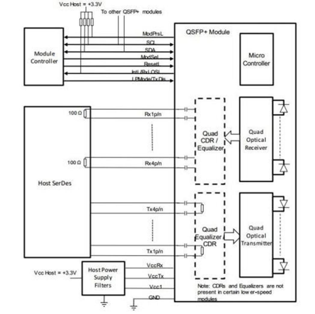
VII. Recommended Interface Circuit

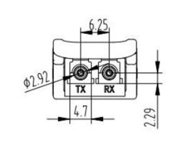
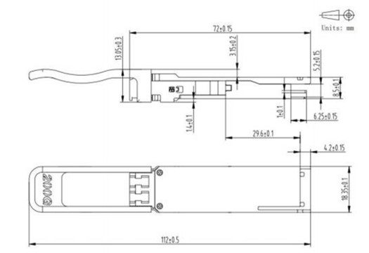
VIII. Mechanical Specifications (Unit:mm)


Want to know about this product?
If you are interested in our products and want to know more details,please leave a message here,we will reply you as soon as we can.