Product Features
1310FPLaser Diode Transmitter
Upto20Kmon9/125μmSMF
3.3Vpower supply
LCduplex optical interface
LVTTLInputs/ Outputs and LVTTL signal detect
Class 1 Laser International Safety Standard IEC 825 Compliant
Operating case temperature range (Standard:0 to +70℃) or(Extended:-40°C to +85°C
Order Information

1.The suffix “N” denotes without Digital diagnostic monitoring
2. The suffix “I” denotes industrial level(The default is commercial-temperature)
Application
RS232/RS485/RS422 receptacle fiber transmission
Otheroptic link
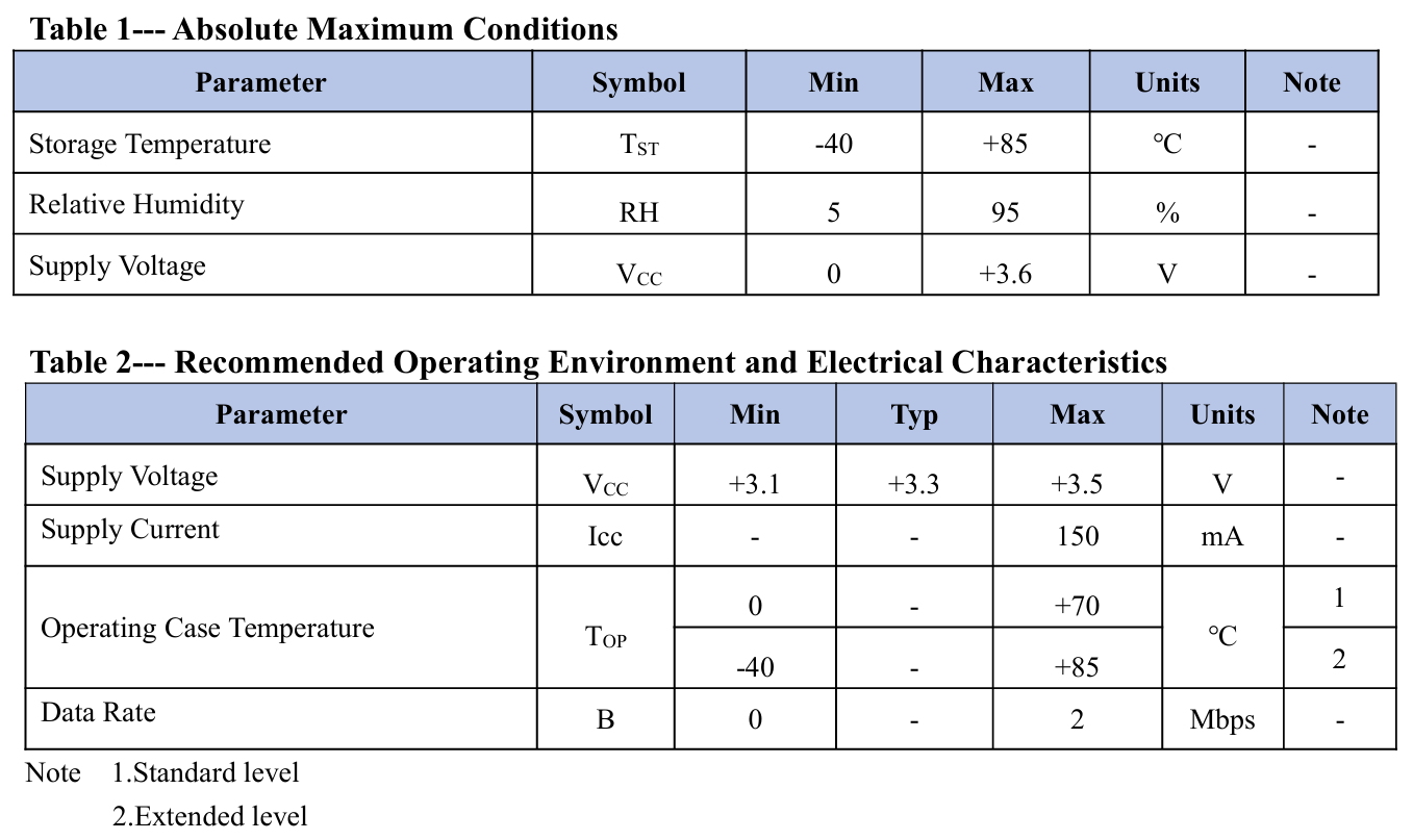
Absolute Maximum Ratings
Operating of the transceiver beyond the Absolute Conditions Listed in Table 1 will degrade or damage the product. It’s not implied that the product would function above the recommended operating environment, it’s possible to reduce the reliability and lifetime of device if Recommended Operating Environment is exceeded (Refer to table 2)
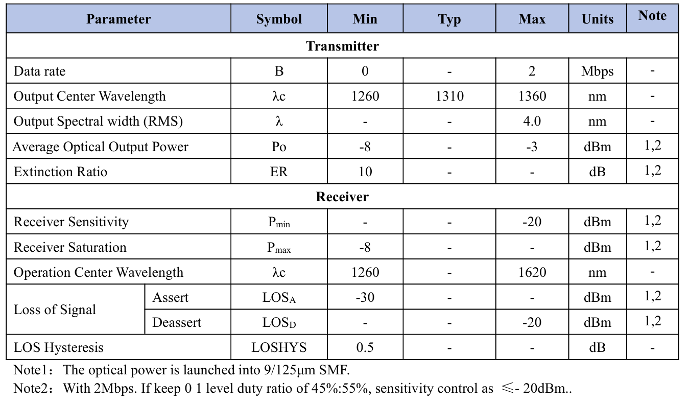
 Optical Parameters
Table3--- ESGALF31-K20C-G Transceiver Optical Characteristics
(Ambient Operating Temperature Ta=+25±5°C, VCC = 3.3±0.2V)
 Pin Definitions
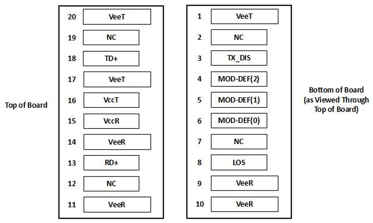
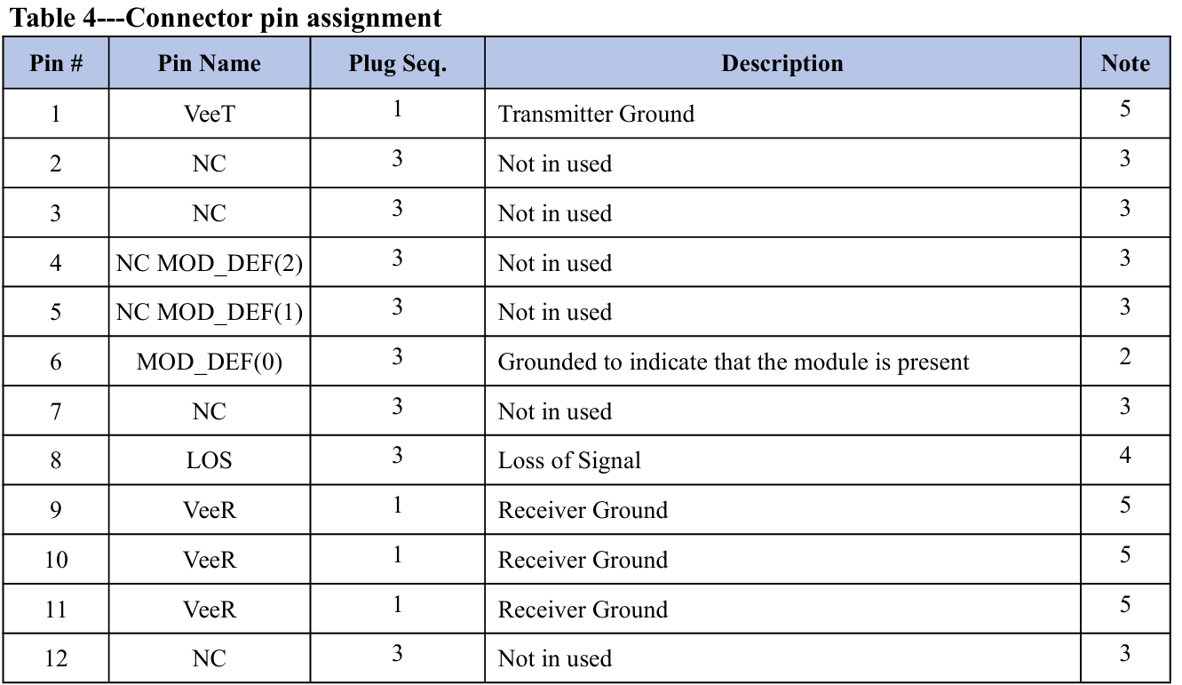
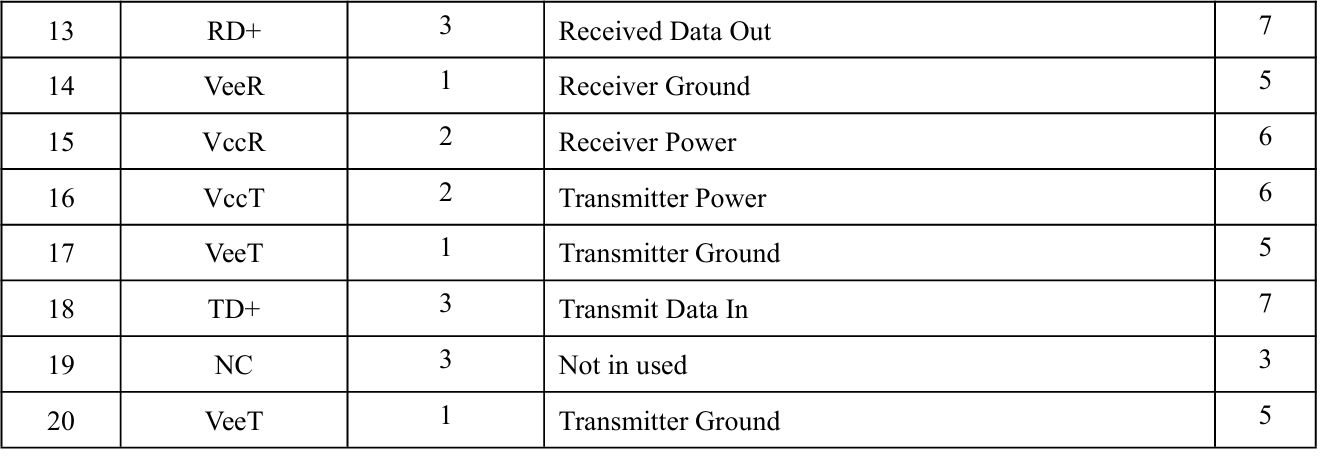 Plug Seq.: Pin engagement sequence during hot plugging.
Note:
1. TX_Disable is an input that is used to shut down the transmitter optical output. Its states are:
Low (0– 0.8V): Transmitter on (>0.8, < 2.0V): Undefined
High (2.0– VCC): Transmitter Disabled
Open: Transmitter Disabled 5
2. Mod-Def 0, 1, 2. These are the module definition pins. They should be pulled up with a 4.7KΩ-10KΩ resistor on the host board. The pull-up voltage shall be VCCT or VCCR.
Mod-Def 0 is grounded by the module to indicate that the module is present
Mod-Def 1 is the clock line of two wire serial interface for serial ID
Mod-Def 2 is the data line of two wire serial interface for serial ID
3. Notin used.
4. LOS (Loss of Signal) is an open collector/drain output, which should be pulled up with a 4.7KΩ-10KΩ resistor. Pull up voltage between 2.0V and VCCT, R+0.3V. When high, this output indicates the received optical power is below the worst-case receiver sensitivity (as defined by the standard in use). Low indicates normal operation. In the low state, the output will be pulled to < 0.8V.
5. VeeRandVeeTmay beinternally connected within the SFP module.
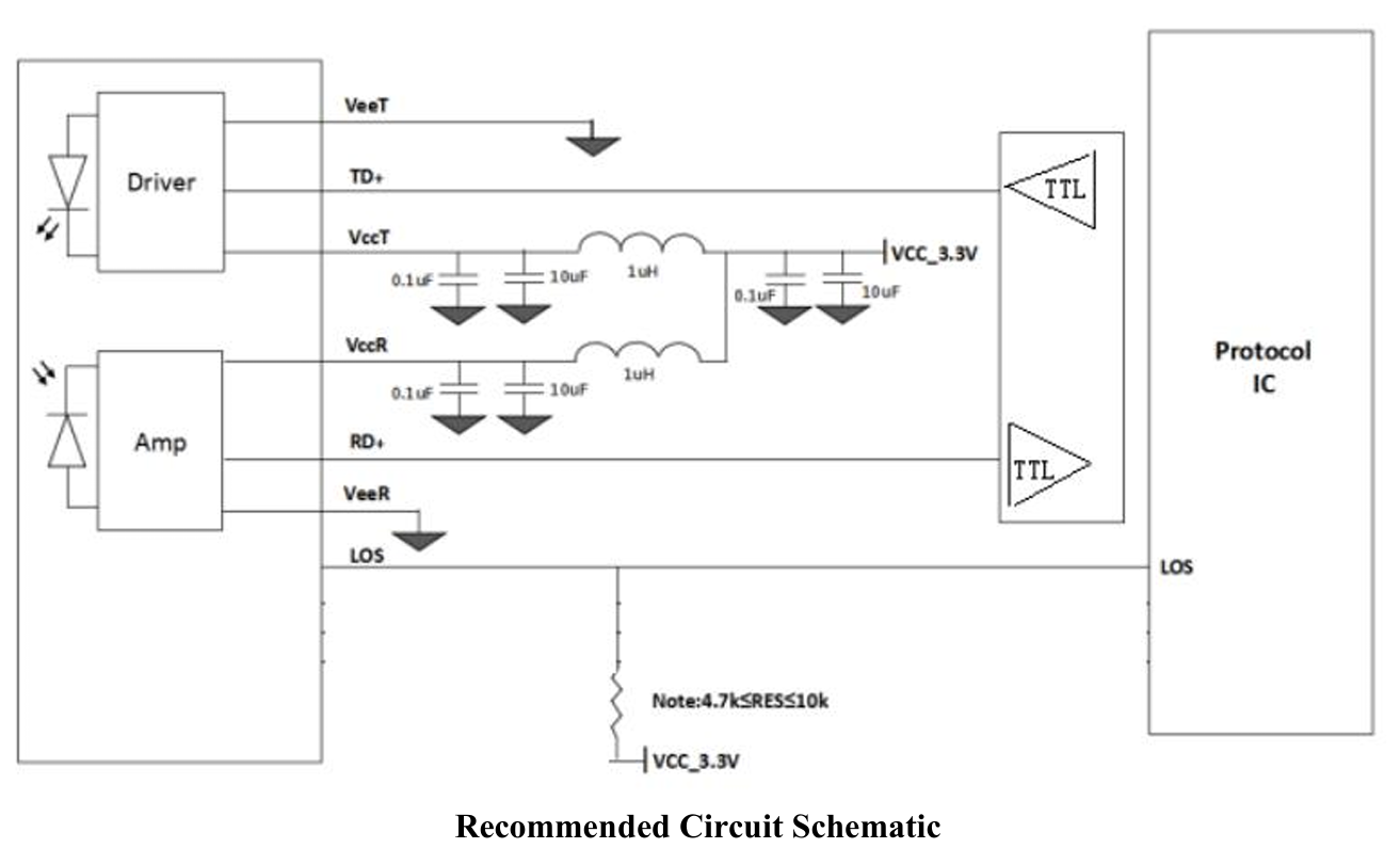
6. VCCR and VCCT are the receiver and transmitter power supplies. They are defined as 3.3V 5% at the SFP connector pin. Maximum supply current is 300 mA. Recommended host board power supply filtering is shown below. Inductors with DC resistance of less than 1 should be used in order to maintain the required voltage at the SFP input pin with 3.3V supply voltage. When the recommended supply filtering network is used, hot plugging of the SFP transceiver module will result in an inrush current of no more than 30 mA greater than the steady state value. VCCR and VCCT may be internally connected within the SFP transceiver module.
7. LVTTLInputs /Outputs
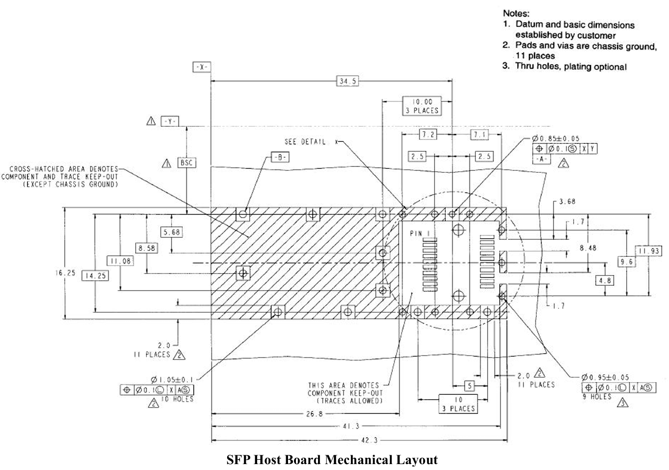
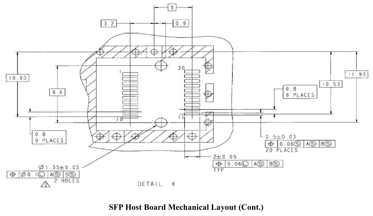
Host Board Layout
Atypical host board mechanical layout for attaching the SFP Connector and Cage System is shown in Figures 1 and 2.
Recommended Circuit Schematic
Module Outline Drawing(Unitsinmm)
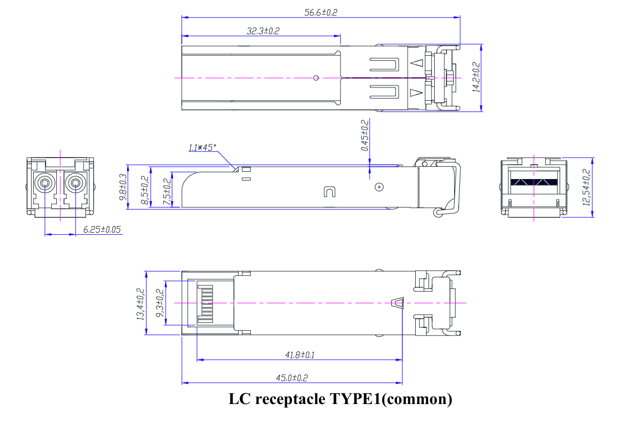
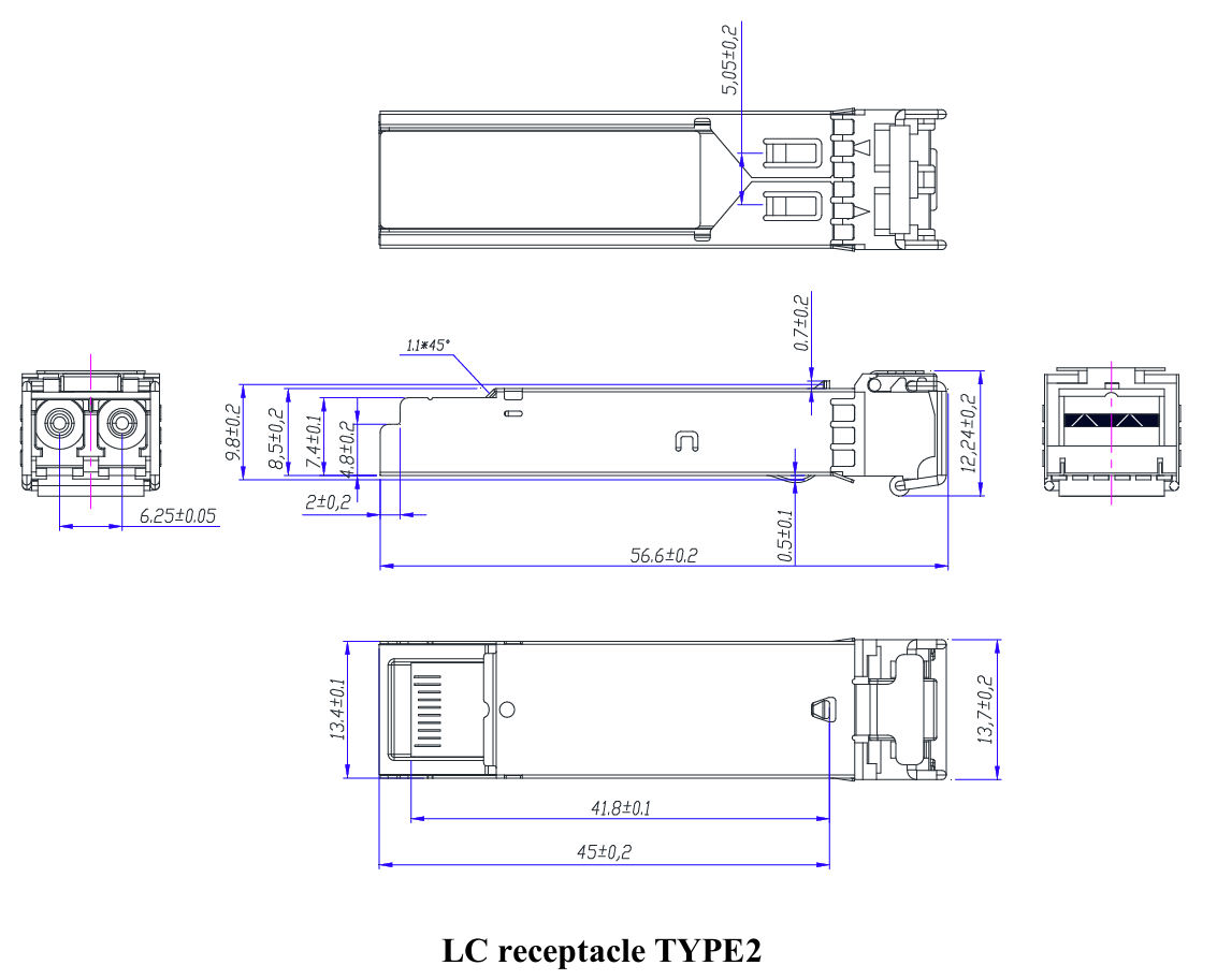
Note:Specificationssubjecttochangewithoutnotice
Want to know about this product?
If you are interested in our products and want to know more details,please leave a message here,we will reply you as soon as we can.