APPLICATIONS
l 400Gb/s Ethernet
l Data Center
l InfiniBand interconnects
l QSFP-DD MSA.
l IEEE802.3bs
l CMIS5.2
Ordering information
|
Part NO. |
Bit Rate (Gbps) |
Laser (nm) |
Distance(m) |
Media |
DDMI |
Connector |
Temp(℃) |
|
ESWSMB31-S50C |
425 |
1310 |
500 |
SMF |
YES |
MPO-12(APC) |
0~70 |
I. General Description
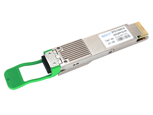
ESWSMB31-S50C is a Sillicon Photonics 400G(4x100G)DR4 transceiver. ESWSMB31-S50C is a fully integrated, 425Gb/s optical transceiver for SMF links up to 500m. ESWSMB31-S50C transmits data in compliance with the optical interface specification IEEEStd802.3-2018 Section 8 400GBASE-DR4. 400GBASE-DR4 specifies the use of 4-level pulse amplitude modulation (PAM4) at 53.125GBand operating at four parallel channels with wavelength on the range of 1304.5-1317.5nm. The bit rate per lane is 106.25Gb/s, which produces an aggregate data rate of 425Gb/s by meas PSM to the transmit ports of the MPO-12 connector. The received optical lanes are paralleled from the receive MPO-12 connector ports to PIN-PD built in PIC (Photonic Integrated Circuit) to recover the PAM4 for interfacing with the electrical interface via with transimpedance amplifier (TIA) surfaced-mounted to PIC.
II. Pin Diagram
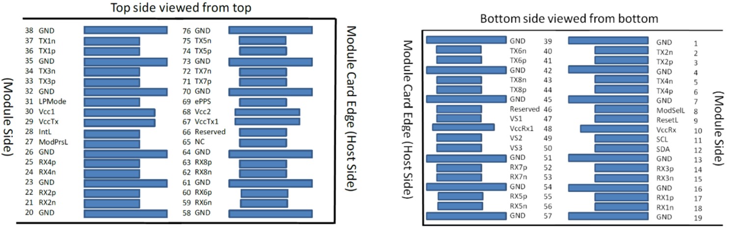
III. Pin Descriptions
|
Pad |
Symbol |
Description |
Ref. |
|
1 |
GND |
Ground |
|
|
2 |
Tx2n |
Transmitter Inverted Data Input |
|
|
3 |
Tx2p |
Transmitter Non-Inverted Data Input |
|
|
4 |
GND |
Ground |
|
|
5 |
Tx4n |
Transmitter Inverted Data Input |
|
|
6 |
Tx4p |
Transmitter Non-Inverted Data Input |
|
|
Pad |
Symbol |
Description |
Ref. |
|
7 |
GND |
Ground |
|
|
8 |
ModSelL |
Module Select |
|
|
9 |
ResetL |
Module Reset |
|
|
10 |
VccRx |
+3.3V Power Supply Receiver |
|
|
11 |
SCL |
2-wire serial interface clock |
|
|
12 |
SDA |
2-wire serial interface data |
|
|
13 |
GND |
Ground |
|
|
14 |
Rx3p |
Receiver Non-Inverted Data Output |
|
|
15 |
Rx3n |
Receiver Inverted Data Output |
|
|
16 |
GND |
Ground |
|
|
17 |
Rx1p |
Receiver Non-Inverted Data Output |
|
|
18 |
Rx1n |
Receiver Inverted Data Output |
|
|
19 |
GND |
Ground |
|
|
20 |
GND |
Ground |
|
|
21 |
Rx2n |
Receiver Inverted Data Output |
|
|
22 |
Rx2p |
Receiver Non-Inverted Data Output |
|
|
23 |
GND |
Ground |
|
|
24 |
Rx4n |
Receiver Inverted Data Output |
|
|
25 |
Rx4p |
Receiver Non-Inverted Data Output |
|
|
26 |
GND |
Ground |
|
|
27 |
ModPrsL |
Module Present |
|
|
28 |
IntL |
Interrupt |
|
|
29 |
VccTx |
+3.3V Power supply transmitter |
|
|
30 |
Vcc1 |
+3.3V Power supply |
|
|
31 |
LPMode |
Low Power mode; |
|
|
32 |
GND |
Ground |
|
|
33 |
Tx3p |
Transmitter Non-Inverted Data Input |
|
|
34 |
Tx3n |
Transmitter Inverted Data Input |
|
|
35 |
GND |
Ground |
|
|
36 |
Tx1p |
Transmitter Non-Inverted Data Input |
|
|
37 |
Tx1n |
Transmitter Inverted Data Input |
|
|
38 |
GND |
Ground |
|
|
39 |
GND |
Ground |
|
|
40 |
Tx6n |
Transmitter Inverted Data Input |
|
|
41 |
Tx6p |
Transmitter Non-Inverted Data Input |
|
|
42 |
GND |
Ground |
|
|
43 |
Tx8n |
Transmitter Inverted Data Input |
|
|
44 |
Tx8p |
Transmitter Non-Inverted Data Input |
|
|
Pad |
Symbol |
Description |
Ref. |
|
45 |
GND |
Ground |
|
|
46 |
Reserved |
For future use |
|
|
47 |
VS1 |
Module Vendor Specific 1 |
|
|
48 |
VccRx1 |
3.3V Power Supply |
|
|
49 |
VS2 |
Module Vendor Specific 2 |
|
|
50 |
VS3 |
Module Vendor Specific 3 |
|
|
51 |
GND |
Ground |
|
|
52 |
Rx7p |
Receiver Non-Inverted Data Output |
|
|
53 |
Rx7n |
Receiver Inverted Data Output |
|
|
54 |
GND |
Ground |
|
|
55 |
Rx5p |
Receiver Non-Inverted Data Output |
|
|
56 |
Rx5n |
Receiver Inverted Data Output |
|
|
57 |
GND |
Ground |
|
|
58 |
GND |
Ground |
|
|
59 |
Rx6n |
Receiver Inverted Data Output |
|
|
60 |
Rx6p |
Receiver Non-Inverted Data Output |
|
|
61 |
GND |
Ground |
|
|
62 |
Rx8n |
Receiver Inverted Data Output |
|
|
63 |
Rx8p |
Receiver Non-Inverted Data Output |
|
|
64 |
GND |
Ground |
|
|
65 |
NC |
No Connect |
|
|
66 |
Reserved |
For future use |
|
|
67 |
VccTx1 |
3.3V Power Supply |
|
|
68 |
Vcc2 |
3.3V Power Supply |
|
|
69 |
Reserved |
For future use |
|
|
70 |
GND |
Ground |
|
|
71 |
Tx7p |
Transmitter Non-Inverted Data Input |
|
|
72 |
Tx7n |
Transmitter Inverted Data Input |
|
|
73 |
GND |
Ground |
|
|
74 |
Tx5p |
Transmitter Non-Inverted Data Input |
|
|
75 |
Tx5n |
Transmitter Inverted Data Input |
|
|
76 |
GND |
Ground |
|
IV. Absolute Maximum Ratings
|
Parameter |
Symbol |
Min. |
Typ. |
Max. |
Unit |
Ref. |
|
Storage Temperature |
TS |
-40 |
|
85 |
ºC |
|
|
Case Operating Temperature |
Top |
0 |
|
70 |
|
|
|
Storage Relative Humidity |
HA |
0 |
|
85 |
% |
1 |
|
Supply Voltage |
VCC |
0 |
|
3.6 |
V |
|
|
Receiver Damage Threshold,per Lane |
PRdmg |
|
|
5.0 |
dBm |
|
Note:
1.Non-condensation.
V. Recommended Operating Conditions
|
Data Rate Spcifications |
Symbol |
Min. |
Typ. |
Max. |
Unit |
Ref. |
|
Power Supply Voltage |
Vcc |
3.135 |
3.3 |
3.465 |
V |
|
|
Bit Rate |
BR |
|
|
425 |
Gbps |
|
|
Operating Case Temperature |
Tc |
0 |
|
70 |
℃ |
|
|
Relative Humidity |
HA |
5 |
|
85 |
% |
1 |
|
Supply Current |
Icc |
|
|
3182 |
mA |
|
|
Total Power Consumption |
PC |
|
|
10.5 |
W |
|
Note:
1.Non-condensation.
VI. Optical Characteristics
|
Parameter |
Symbol |
Min. |
Typ. |
Max. |
Unit |
Ref. |
|
|
Transmitter(per lane) |
|||||||
|
Channel data rate |
FDC |
106.25 |
Gb/s |
|
|||
|
Data rate per lane |
FSG |
53.125 |
Gb/s |
PAM4 |
|||
|
Center Wavelength |
λC |
1304.5 |
1311 |
1317.5 |
nm |
|
|
|
RMS Spectral Width |
σ |
|
|
0.6 |
nm |
1 |
|
|
Receiver(per lane) |
|||||||
|
Damage threshold |
|
5 |
|
|
dBm |
2 |
|
|
Average receive power, each lane |
|
–5.9 |
|
4.0 |
dBm |
3 |
|
|
Receiver reflectance |
Rr |
|
|
-26 |
dB |
|
|
|
Receiver sensitivity(OMA outer), each lane |
SEN |
Max(-3.9,SECQ-5.3) |
dBm |
4 |
|||
|
Stressed receiver sensitivity (OMA outer), each lane |
SRS |
|
|
-1.9 |
dBm |
|
|
|
Receiver Loss of Signal Indicator Assert Level |
LOSA |
-15 |
|
-7.9 |
dBm |
|
|
|
Receiver Loss of Signal Indicator De-assert Level |
LOSD |
|
|
-7.5 |
dBm |
|
|
|
Hysteresis |
LOSH |
0.5 |
|
5 |
dB |
|
|
Notes:
1. RMS spectral width is the standard deviation of the spectrum.
2. The receiver shall be able to tolerate, without damage, continuous exposure to an optical input signal having this average power level on one lane. The receiver does not have to operate correctly at this input power.
3. Average receive power, each lane (min) is not the principal indicator of signal strength. A received power below this value cannot be compliant; however, a value above this does not ensure compliance.
4. Receiver sensitivity is informative and is defined for a transmitter with a value of SECQ. Measured with conformance test signal at TP3 for BER=2.4E-4 Pre-FEC.
VII. Electrical Interface Characteristics
|
Parameter |
Symbol |
Min. |
Typ. |
Max. |
Unit |
Ref. |
|
Supply Voltage |
VCC1, VCCTX, VCCRX |
3.135 |
|
3.465 |
V |
|
|
Power Dissipation |
Pd |
|
|
10.5 |
W |
|
|
Transmitter(per Lane) |
||||||
|
Input different impedance |
Rin |
90 |
100 |
110 |
Ω |
|
|
Input Logic Level High |
- |
2 |
|
Vcc |
V |
|
|
Input Logic Level Low |
- |
0 |
|
0.8 |
V |
|
|
Differential data input swing |
Vin,pp |
|
|
880 |
mVpp |
|
|
Receiver (per Lane) |
||||||
|
Error Bit Rate |
BER |
|
|
2.4E-4 |
|
|
|
Output different impedance |
Rout |
90 |
100 |
110 |
Ω |
|
|
Output Logic Level High |
- |
Vcc-0.5 |
|
Vcc |
V |
|
|
Output Logic Level Low |
- |
0 |
|
0.4 |
V |
|
|
Differential data Output swing |
Vout,pp |
|
|
900 |
mVpp |
|
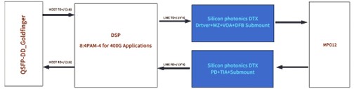
VIII.Functional Block Didgram
IX. Digital Diagnostic Monitor Accuracy
The following characteristics are defined over recommended operating conditions.
|
Parameter |
Accuracy |
Unit |
|
Internally Measured Transceiver Temperature |
+/-3 |
℃ |
|
Internally Messured Transceiver Supply Voltage |
+/-3 |
% |
|
Measured Tx Bias Current |
+/-10 |
% |
|
Measured Tx Output Power |
+/-3 |
dB |
|
Measured Rx Received Average Optical Power |
+/-3 |
dB |
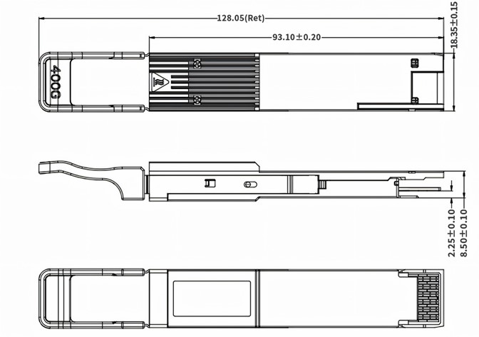
X. Mechanical Specifications (Unit: mm)
Want to know about this product?
If you are interested in our products and want to know more details,please leave a message here,we will reply you as soon as we can.
 LPWSLC23-K02C
 LPWSAA31-M(L)xxC

Address : East of 2F, Tianmen Optical Valley Science Park,Qiaoxiang Economic development area,Tianmen, Hubei Province.
Tel : 15012662571
Email : chris.peng@talptech.com
Skype : 15012662571