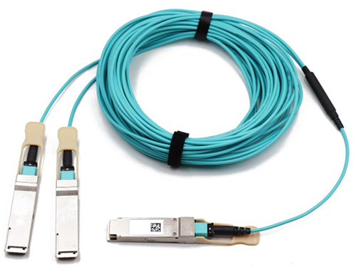
APPLICATIONS
l 200Gb/s InfiniBand HDR systems
l Other optical links
Compliance
l QSFP MSA.
l IEEE802.3cd
l SFF-8636
l RoHS
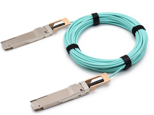
Ordering information
|
Package |
Product part NO. |
Distance |
Temperature Range |
|
QSFP56 |
ESCRAA32-M01C |
1-metercable |
Commercial: 0~70℃ |
|
QSFP56 |
ESCRAA32-M03C |
3-metercable |
Commercial: 0~70℃ |
|
QSFP56 |
ESCRAA32-M05C |
5-metercable |
Commercial: 0~70℃ |
|
QSFP56 |
ESCRAA32-M07C |
7-metercable |
Commercial: 0~70℃ |
|
QSFP56 |
ESCRAA32-M10C |
10-metercable |
Commercial: 0~70℃ |
|
QSFP56 |
ESCRAA32-M15C |
15-metercable |
Commercial: 0~70℃ |
|
QSFP56 |
ESCRAA32-M20C |
20-metercable |
Commercial: 0~70℃ |
|
QSFP56 |
ESCRAA32-M30C |
30-metercable |
Commercial: 0~70℃ |
|
*For availability of additional cable lengths, please contact Esion.
|
|||
I. Pin Diagram
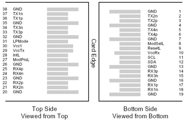
II. Pin Descriptions
|
Pin |
Logic |
Symbol |
Name/Description |
Ref. |
|
1 |
|
GND |
Ground |
1 |
|
2 |
CML-I |
Tx2n |
Transmitter Inverted Data Input |
|
|
3 |
CML-I |
Tx2p |
Transmitter Non-Inverted Data Input |
|
|
4 |
|
GND |
Ground |
1 |
|
5 |
CML-I |
Tx4n |
Transmitter Inverted Data Input |
|
|
6 |
CML-I |
Tx4p |
Transmitter Non-Inverted Data Input |
|
|
7 |
|
GND |
Ground |
1 |
|
8 |
LVTTL-I |
ModSe1L |
Module Select |
|
|
9 |
LVTTL-I |
ResetL |
Module Reset |
|
|
10 |
|
Vcc Rx |
+3.3V Power supply receiver |
|
|
11 |
LVCMOS-I |
SCL |
2-wire serial interface clock |
|
|
12 |
LVCMOS-I/O |
SDA |
2-wire serial interface data |
|
|
13 |
|
GND |
Ground |
1 |
|
14 |
CML-O |
Rx3p |
Receiver Non-Inverted Data Output |
|
|
15 |
CML-O |
Rx3n |
Receiver Inverted Data Output |
|
|
16 |
|
GND |
Ground |
1 |
|
17 |
CML-O |
Rx1p |
Receiver Non-Inverted Data Output |
|
|
18 |
CML-O |
Rx1n |
Receiver Inverted Data Output |
|
|
19 |
|
GND |
Ground |
1 |
|
20 |
|
GND |
Ground |
1 |
|
21 |
CML-O |
Rx2n |
Receiver Inverted Data Output |
|
|
22 |
CML-O |
Rx2p |
Receiver Non-Inverted Data Output |
|
|
23 |
|
GND |
Ground |
1 |
|
24 |
CML-O |
Rx4n |
Receiver Inverted Data Output |
|
|
25 |
CML-O |
Rx4p |
Receiver Non-Inverted Data Output |
|
|
26 |
|
GND |
Ground |
1 |
|
27 |
LVTTL-O |
ModPrSL |
Module Present |
|
|
28 |
LVTTL-O |
IntL |
Interrupt |
|
|
29 |
|
Vcc Tx |
+3.3V Power supply transmitter |
|
|
30 |
|
Vcc1 |
+3.3V Power Supply |
|
|
31 |
LVTTL-I |
LPMode |
Low Power Mode |
|
|
32 |
|
GND |
Ground |
1 |
|
33 |
CML-I |
Tx3p |
Transmitter Non-Inverted Data Input |
|
|
34 |
CML-I |
Tx3n |
Transmitter Inverted Data Input |
|
|
35 |
|
GND |
Ground |
1 |
|
36 |
CML-I |
Tx1p |
Transmitter Non-Inverted Data Input |
|
|
37 |
CML-I |
Tx1n |
Transmitter Inverted Data Input |
|
|
38 |
|
GND |
Ground |
1 |
Note:
1. Circuit ground is internally isolated from chassis ground.
III. Absolute Maximum Ratings
|
Parameter |
Symbol |
Min. |
Typ. |
Max. |
Unit |
Ref. |
|
Storage Temperature |
TS |
-40 |
|
85 |
ºC |
|
|
Storage Ambient Humidity |
HA |
0 |
|
85 |
% |
|
|
Maximum Supply Voltage |
VCC |
-0.5 |
|
3.6 |
V |
|
|
Lead Soldering Temperature/Time |
TSOLD |
|
|
260/10 |
ºC/sec |
1 |
|
Lead Soldering Temperature/Time |
TSOLD |
|
|
360/10 |
ºC/sec |
2 |
Note:
1.Suitable for wave soldering.
2. Only for soldering by iron.
IV. Recommended Operating Conditions
|
Data Rate Spcifications |
Symbol |
Min. |
Typ. |
Max. |
Unit |
Ref. |
|
Supply Voltage |
Vcc |
3.13 |
3.3 |
3.47 |
V |
|
|
Baud Rate(per channel ) PAM4 |
BR |
|
26.5625 |
|
GBd |
1 |
|
Operating Case Temperature |
Tc |
0 |
|
70 |
℃ |
|
Notes:
1. Supports 200GBASE-SR4 per IEEE 802.3cd.
V. Electrical Interface Characteristics
|
Parameter |
Symbol |
Min. |
Typ. |
Max. |
Unit |
Ref. |
|
Supply Voltage |
VCC1, VCCTX, VCCRX |
3.15 |
|
3.45 |
V |
|
|
Power Dissipation (100GbE retiming on all lanes) |
Pd100G |
|
|
4.5 |
W |
|
|
Power Dissipation (50GbE retiming on all lanes) |
Pd50G |
|
|
2.5 |
W |
|
|
Transmitter(per Lane) |
||||||
|
Input different impedance |
Rin |
90 |
100 |
110 |
Ω |
|
|
Single ended input voltage tolerance |
VinT |
-0.3 |
|
4.0 |
V |
|
|
Differential Input Voltage Amplitude |
Vin,pp |
|
|
900 |
mV |
|
|
Receiver (per Lane) |
||||||
|
Error Bit Rate |
BER |
|
|
2.4E-4 |
|
|
|
Output different impedance |
Rout |
90 |
100 |
110 |
Ω |
|
|
Single-ended output voltage |
VoutR |
-0.3 |
|
4.0 |
V |
|
|
Differential Output Voltage Amplitude |
Vout,pp |
|
|
900 |
mV |
|
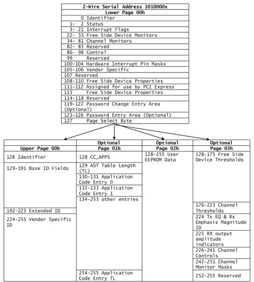
VI. Digital Diagnostic Functions
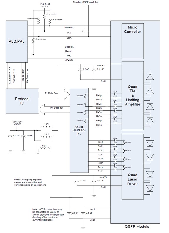
VII. Recommended Interface Circuit
VIII.Mechanical Specifications (Unit: mm)
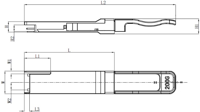
Unit mm
|
|
L |
L1 |
L2 |
L3 |
W |
W1 |
W2 |
H |
H1 |
H2 |
|
Max |
72.2 |
- |
- |
4.35 |
18.45 |
- |
6.2 |
8.6 |
12.0 |
5.35 |
|
Type |
72.0 |
- |
121 |
4.20 |
18.35 |
- |
- |
8.5 |
11.8 |
5.2 |
|
Min |
68.8 |
16.5 |
- |
4.05 |
18.25 |
2.2 |
5.8 |
8.4 |
11.6 |
5.05 |
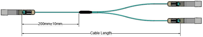
Cable Length
|
Parameter |
Value |
Units |
|
Diameter |
3±0.2 |
mm |
|
Minimum bend radius |
30 |
mm |
|
Length tolerance |
1≤Length≤4.5m: +20/-0 |
cm |
|
5≤Length≤14.5m: +40/-0 |
cm |
|
|
Length≥15.0m: +3/-0% |
m |
|
|
Cable color |
Aqua(OM3) |
|
Want to know about this product?
If you are interested in our products and want to know more details,please leave a message here,we will reply you as soon as we can.
 LPCRLB31-K02C
 LPCRAA31-M(L)xxC

Address : East of 2F, Tianmen Optical Valley Science Park,Qiaoxiang Economic development area,Tianmen, Hubei Province.
Tel : 15012662571
Email : chris.peng@talptech.com
Skype : 15012662571