Applications
● 400G Ethernet
● Data center network
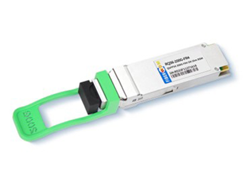
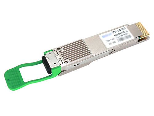
ESWSLC23-K02C is a transceiver module designed for 2 km optical communication applications, and it is compliant with 100G Lambda MSA standard. This module can convert 8-channel 53.125 Gbps electrical data to 4-channel 106.25 Gbps optical signals, and multiplex them into a single channel for 425 Gbps optical transmission. Similarly, it optically de-multiplexes a 425 Gbps input into 4-channel signals, and converts them to 8-channel output electrical data on the receiver side. It has been designed to meet the harshest external operating conditions including temperature, humidity and EMI interference. The module offers very high functionality and feature integration, accessible via the I2C interface.
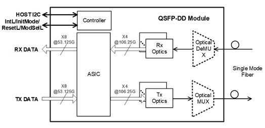
Figure 1-1 Transceiver block diagram
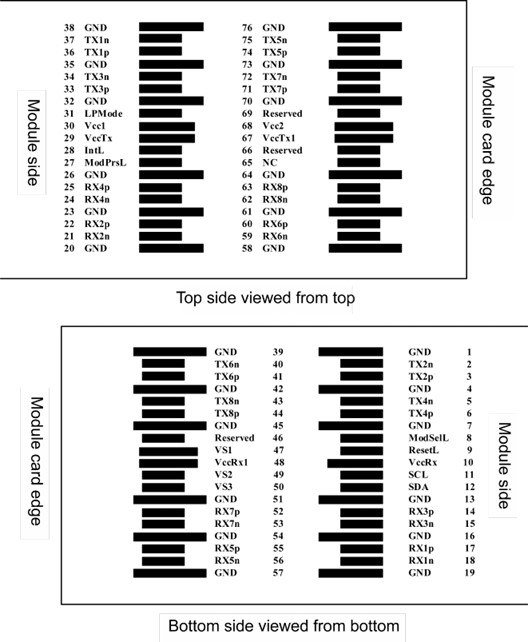
Pin
Logic
Symbol
Description
Plug sequence
Notes
1
GND
Ground
1B
1
2
CML-I
Tx2n
Transmitter Inverted Data Input
3B
3
CML-I
Tx2p
Transmitter Non-Inverted
Data
3B
Pin
Logic
Symbol
Description
Plug sequence
Notes
Input
4
GND
Ground
1B
1
5
CML-I
Tx4n
Transmitter Inverted Data Input
3B
6
CML-I
Tx4p
Transmitter Non-Inverted
Data Input
3B
7
GND
Ground
1B
1
8
LVTTL-I
ModSelL
Module Select
3B
9
LVTTL-I
ResetL
Module Reset
3B
10
VccRx
+3.3 V Power Supply
Receiver
2B
2
11
LVCMOS-
I/O
SCL
2-wire Serial Interface
Clock
3B
12
LVCMOS-
I/O
SDA
2-wire Serial Interface
Data
3B
13
GND
Ground
1B
1
14
CML-O
Rx3p
Receiver Non-Inverted Data Output
3B
15
CML-O
Rx3n
Receiver Inverted Data Output
3B
16
GND
Ground
1B
1
17
CML-O
Rx1p
Receiver Non-Inverted Data
Output
3B
18
CML-O
Rx1n
Receiver Inverted Data Output
3B
19
GND
Ground
1B
1
20
GND
Ground
1B
1
21
CML-O
Rx2n
Receiver Inverted Data
Output
3B
22
CML-O
Rx2p
Receiver Non-Inverted Data Output
3B
23
GND
Ground
1B
1
24
CML-O
Rx4n
Receiver Inverted Data Output
3B
25
CML-O
Rx4p
Receiver Non-Inverted Data Output
3B
26
GND
Ground
1B
1
27
LVTTL-I
ModPrsL
Module Present
3B
28
LVTTL-I
IntL
Interrupt
3B
29
VccTx
+3.3 V Power Supply Transmitter
2B
2
30
Vcc1
+3.3 V Power Supply
2B
2
31
LVTTL-I
InitMode
Initialization Mode; In
legacy QSFP applications, the InitMode pad is
3B
Pin
Logic
Symbol
Description
Plug sequence
Notes
called LPMODE
32
GND
Ground
1B
1
33
CML-I
Tx3p
Transmitter Non-Inverted
Data Input
3B
34
CML-I
Tx3n
Transmitter Inverted Data Input
3B
35
GND
Ground
1B
1
36
CML-I
Tx1p
Transmitter Non-Inverted
Data Input
3B
37
CML-I
Tx1n
Transmitter Inverted Data
Input
3B
38
GND
Ground
1B
1
39
GND
Ground
1A
1
40
CML-I
Tx6n
Transmitter Inverted Data Input
3A
41
CML-I
Tx6p
Transmitter Non-Inverted
Data Input
3A
42
GND
Ground
1A
1
43
CML-I
Tx8n
Transmitter Inverted Data Input
3A
44
CML-I
Tx8p
Transmitter Non-Inverted
Data Input
3A
45
GND
Ground
1A
1
46
Reserved
For future use
3A
3
47
VS1
Module Vendor Specific 1
3A
3
48
VccRx1
+3.3 V Power supply
2A
2
49
VS2
Module Vendor Specific 2
3A
3
50
VS3
Module Vendor Specific 3
3A
3
51
GND
Ground
1A
1
52
CML-O
Rx7p
Receiver Non-Inverted Data Output
3A
53
CML-O
Rx7n
Receiver Inverted Data Output
3A
54
GND
Ground
1A
1
55
CML-O
Rx5p
Receiver Non-Inverted Data Output
3A
56
CML-O
Rx5n
Receiver Inverted Data Output
3A
57
GND
Ground
1A
1
58
GND
Ground
1A
1
59
CML-O
Rx6n
Receiver Inverted Data
Output
3A
Pin
Logic
Symbol
Description
Plug sequence
Notes
60
CML-O
Rx6p
Receiver Non-Inverted Data
Output
3A
61
GND
Ground
1A
1
62
CML-O
Rx8n
Receiver Inverted Data
Output
3A
63
CML-O
Rx8p
Receiver Non-Inverted Data Output
3A
64
GND
Ground
1A
1
65
NC
No Connect
3A
3
66
Reserved
For Future Use
3A
3
67
VccTx1
+3.3 V Power Supply
2A
2
68
Vcc2
+3.3 V Power Supply
2A
2
69
Reserved/(ep ps)
Precision Time Protocol
(PTP) Reference Clock Input
3A
3
70
GND
Ground
1A
1
71
CML-I
Tx7p
Transmitter Non-Inverted
Data Input
3A
72
CML-I
Tx7n
Transmitter Inverted Data Input
3A
73
GND
Ground
1A
1
74
CML-I
Tx5p
Transmitter Non-Inverted
Data Input
3A
75
CML-I
Tx5n
Transmitter Inverted Data Input
3A
76
GND
Ground
1A
1
Note:
1. QSFP-DD uses common ground (GND) for all signals and supply (power). All are common within the QSFP-DD module and all module voltages are referenced to this potential unless otherwise noted. Connect these directly to the host board signal-common ground plane.
2. VccRx, VccRx1, Vcc1, Vcc2, VccTx and VccTx1 shall be applied concurrently. Requirements defined for the host side of the Host Card Edge Connector are listed in the table. VccRx, VccRx1, Vcc1, Vcc2, VccTx and VccTx1 may be internally connected within the module in any combination. The connector Vcc pins are each rated for a maximum current of 1000 mA.
3. All Vendor Specific, Reserved and No Connect pins may be terminated with 50 Ω to ground on the host. Pad 65 (No Connect) shall be left unconnected within the module. Vendor specific and Reserved pads shall have an impedance to GND that is greater than 10 kΩ and less than 100 pF.
4. Plug Sequence specifies the mating sequence of the host connector and module.
It has to be noted that the operation in excess of any individual absolute maximum ratings might cause permanent damage to this module.
Parameter
Symbol
Min.
Typ.
Max.
Unit
Notes
Maximum supply voltage
Vcc
–0.3
3.3
3.6
V
Storage temperature
Ts
–40
85
°C
Relative humidity
RH
0
85
%
Electrical and optical characteristics below are defined under this operating environment, unless otherwise specified.
Parameter
Symbol
Min.
Typ.
Max.
Unit
Notes
Supply voltage
Vcc
3.135
3.3
3.465
V
Case temperature
T
0
70
°C
Data rate accuracy
–100
100
ppm
Link distance
0.5
2000
m
1
Note:
1. G.652 Single-mode optical fiber.
|
Parameter |
Min. |
Typ. |
Max. |
Unit |
Notes |
|
Power dissipation |
|
|
12 |
W |
|
|
Supply current |
|
|
3.63 |
A |
|
|
Receiver (module input) |
|||||
|
Data rate, each lane |
26.5625 ± 100 ppm |
GBd |
|
||
|
Overload differential voltage pk-pk |
900 |
|
|
mV |
|
|
Common mode voltage |
–350 |
|
2850 |
mV |
|
|
Parameter |
Min. |
Typ. |
Max. |
Unit |
Notes |
|
Differential termination resistance mismatch |
|
|
10 |
% |
At 1 MHz |
|
Differential return loss (SDD11) |
Equation (16-1) |
dB |
OIF-CEI- 56G-VSR- PAM4 |
||
|
Common mode to differential mode conversion (SCD11) |
Equation (16-2) |
dB |
OIF-CEI- 56G-VSR- PAM4 |
||
|
Stressed input test |
See OIF-CEI-56G-VSR-PAM4 Section 16.3.10.3 |
|
|
||
|
Transmitter (module output) |
|||||
|
Data rate, each lane |
26.5625 ± 100 ppm |
GBd |
|
||
|
Differential voltage, pk-pk |
|
|
900 |
mV |
|
|
Common mode voltage (Vcm) |
–350 |
|
2850 |
mV |
|
|
Common mode noise, RMS |
|
|
17.5 |
mV |
|
|
Differential termination resistance mismatch |
|
|
10 |
% |
At 1 MHz |
|
Differential return loss (SDD22) |
|
|
Equation (16-1) |
dB |
|
|
Common mode to differential mode conversion (SDC22) |
|
|
Equation (16-3) |
dB |
|
|
Common mode return loss (SCC22) |
|
|
–2 |
dB |
From 250 MHz to fb GHz |
|
Transition time |
9.5 |
|
|
ps |
|
|
Near-end eye width at 10-6 probability (EW6) |
0.265 |
|
|
UI |
|
|
Near-end eye height at 10-6 probability (EH6) |
70 |
|
|
mV |
|
|
Far-end eye width at 10-6 probability (EW6) |
0.20 |
|
|
UI |
|
|
Far-end eye height at 10-6 probability (EH6) |
30 |
|
|
mV |
|
|
Near-end eye linearity |
0.85 |
|
|
|
|
|
Parameters |
Unit |
Min. |
Typ. |
Max. |
|
Transmitter |
||||
|
Data rate, each Lane |
GBd |
53.125 ± 100 ppm |
||
|
Modulation format |
|
PAM4 |
||
|
Line wavelengths |
nm |
1264.5 |
1271 |
1277.5 |
|
1284.5 |
1291 |
1297.5 |
||
|
1304.5 |
1311 |
1317.5 |
||
|
1324.5 |
1331 |
1337.5 |
||
|
Total average launch power |
dBm |
|
|
9.5 |
|
Average launch power, each lane |
dBm |
–3.3 |
|
3.5 |
|
Optical modulation amplitude (OMA), each lane |
dBm |
–0.2 |
|
3.7 |
|
Extinction ratio (ER) |
dB |
3.5 |
|
|
|
Side-mode suppression ratio (SMSR) |
dB |
30 |
|
|
|
Launch power in OMA minus TDECQ, each lane, for ER ≥ 4.5 dB |
dB |
–1.7 |
|
|
|
Launch power in OMA minus TDECQ, each lane, for ER < 4.5 dB |
dBm |
–1.6 |
|
|
|
Transmitter and dispersion eye closure for PAM4, each Lane (TDECQ) |
dB |
|
|
3.4 |
|
Difference in launch power between any two lanes (OMA outer) |
dB |
|
|
4 |
|
RIN17.1OMA |
dB/Hz |
|
|
–136 |
|
Optical return loss tolerance |
dB |
|
|
17.1 |
|
Transmitter reflectance |
dB |
|
|
–26 |
|
Parameters |
Unit |
Min. |
Typ. |
Max. |
|
Average launch power of OFF transmitter, each Lane |
dBm |
|
|
–20 |
|
Receiver |
||||
|
Data rate, each Lane |
GBd |
53.125 ± 100 ppm |
||
|
Modulation format |
|
PAM4 |
||
|
Damage threshold, each lane |
dBm |
4.5 |
|
|
|
Line wavelengths |
nm |
1264.5 |
1271 |
1277.5 |
|
1284.5 |
1291 |
1297.5 |
||
|
1304.5 |
1311 |
1317.5 |
||
|
1324.5 |
1331 |
1337.5 |
||
|
Average receiver power, each lane |
dBm |
–7.3 |
|
3.5 |
|
Receiver power, each lane (OMA) |
dBm |
|
|
3.7 |
|
Difference in receiver power between any two lanes (OMA) |
dB |
|
|
4.1 |
|
Receiver sensitivity (OMA outer) , each lane (max) |
dBm |
See Note |
||
|
LOS assert |
dBm |
–20 |
|
|
|
LOS deassert |
dBm |
|
|
–8.6 |
|
LOS hysteresis |
dB |
0.5 |
|
|
|
Receiver reflectance |
dB |
|
|
–26 |
|
Conditions of stressed receiver sensitivity |
||||
|
Stressed eye closure for PAM4 (SECQ), lane under test |
dB |
0.9 |
|
3.4 |
|
OMA outer of each aggressor lane |
dBm |
|
1.5 |
|
|
Long term performance test |
||||
|
BER FLOOR |
|
1E – 6 @ –3.1 ~ 2 dBm |
||
Note:
Measured with conformance test signal for BER = 2.4 x 10 - 4. A compliant receiver shall have stressed receiver sensitivity (OMA outer), each lane values below the mask of Figure 6-1, for SECQ values between 0.9 and 3.4 dB.
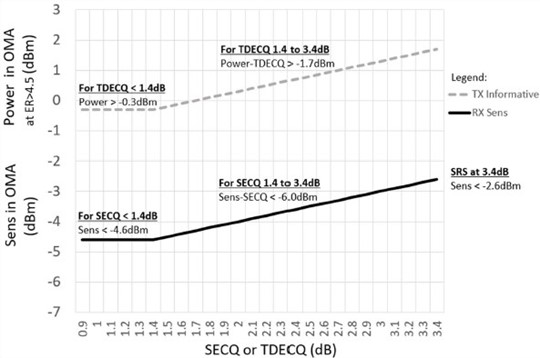
Figure 6-1
Stressed receiver sensitivity mask for 400GE-FR4
Digital diagnostic management interface (DDMI) is realized by I2C interface in compliance with CMIS 4.0. diagnostic management functions are realized, and the data addresses are listed in the form below.
|
Performance item |
Data address |
|
|
|
|
Alarm & Warning |
Alarm & Warning thresholds |
Monitor |
|
Module temperature |
Lower page 9 |
Page2h (128-135) |
Lower page (14-15) |
|
Module voltage |
Lower page 9 |
Page2h (136-143) |
Lower page (16-17) |
|
Bias current |
Page11h (143-146) |
Page2h (184-191) |
Page11h (170-177) |
|
Transmitter optical power |
Page11h (139-142) |
Page2h (176-183) |
Page11h (154-161) |
|
Receiver optical power |
Page11h (149-152) |
Page2h (192-199) |
Page11h (186-193) |
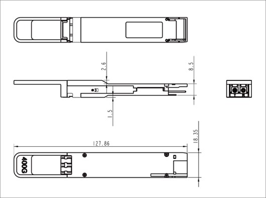
Figure 8-1 OM3660FX102 mechanical dimensions
|
Feature |
Agency |
Standard |
Performance |
|
Safety |
NRTL |
UL 62368-1 CAN/CSA C22.2 No. 62368-1 IEC 60825-1 IEC 60825-2 |
NRTL recognized component for US and CAN |
|
TUV |
EN 62368-1 EN 60825-1 EN 60825-2 |
TUV certificate |
|
|
FDA |
U.S. 21 CFR 1040.10 & 1040.11 |
FDA/CDRH certified with accession number according to Laser Notice 56 |
|
|
Electromagnetic |
Radiated |
EMC Directive 2014/30/EU |
Class B digital device with a minimum –6 dB margin to the |
|
Feature |
Agency |
Standard |
Performance |
|
Compatibility |
emissions |
EN 55032 CISPR 32 FCC rules 47 CFR Part 15 ICES-003 VCCI-CISPR 32 AS/NZS CISPR 32 |
limit when tested with a metal enclosure. Final margin may vary depending on system application, good system EMI design practice, ie: suitable metal enclosure and well- bonding, is required to achieve Class B margins at the system level. Tested frequency range: 30 MHz to 40 GHz or 5th harmonic (5 times the highest frequency), whichever is less. |
|
ESD |
EMC Directive 2014/30/EU EN 55035 CISPR 35 IEC/EN 61000-4-2 |
Withstands discharges of ± 8 kV contact, ±15 kV air. |
|
|
Radiated immunity |
EMC Directive 2014/30/EU EN 55035 CISPR 35 IEC/EN 61000-4-3 |
Field strength of 10 V/m from 80 MHz to 6 GHz. |
|
|
Restriction of Hazardous Substances |
RoHS |
EU RoHS (2011/65/EU & (EU) 2015/863) & UK RoHS EN IEC 63000:2018 & BS EN IEC 63000:2018 |
|
Normal ESD precautions are required during the handling of this module. This transceiver is shipped in ESD protective packaging. It should be removed from the packaging and otherwise handled in an ESD protected environment utilizing standard grounded benches, floor mats, and wrist straps.
|
Parameter |
Threshold value |
Notes |
|
ESD of high-speed pins |
1 kV |
Human Body Model |
|
ESD of low-speed pins |
2 kV |
Human Body Model |
|
Air discharge during operation |
15 kV |
|
|
Direct contact discharges to the case |
8 kV |
|
Do not look into fiber end faces without eye protection using an optical meter (such as magnifier and microscope) within 100 mm, unless you ensure that the laser output is disabled. When operating an optical meter, observe the operation requirements.
CAUTION–Use of controls or adjustments or performance of procedures other than those specified herein may result in hazardous radiation exposure.
Attention–L'utilisation des commandes ou réglages ou l'exécution des procédures autres que celles spécifiées dans les présentes exigences peuvent être la cause d'une exposition à un rayonnement dangereux.
|
Part NO. |
Bit Rate (Gbps) |
Laser (nm) |
Distance(km) |
Media |
DDMI |
Connector |
Temp(℃) |
|
LPWSLC23-K02C |
425 |
1271; 1291; 1311; 1331 |
2 |
Single-mode fiber |
YES |
LC |
0~70 |
Want to know about this product?
If you are interested in our products and want to know more details,please leave a message here,we will reply you as soon as we can.
 LPWSMB31-S50C
 LPWSAA31-M(L)xxC

Address : East of 2F, Tianmen Optical Valley Science Park,Qiaoxiang Economic development area,Tianmen, Hubei Province.
Tel : 15012662571
Email : chris.peng@talptech.com
Skype : 15012662571