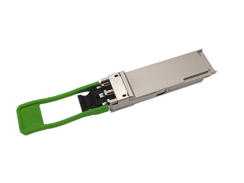
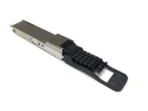
APPLICATIONS
l 100Gigabit Ethernet
Compliance
l QSFP28 MSA.
l IEEE802.3bm
l SFF-8636
l RoHS
Ordering information
|
Part No. |
Bit Rate (Gbps) |
Laser (nm) |
Distance |
Fiber Type |
DDMI |
Connector |
Temp |
|
ESBQLC23-K02C |
4*25.78125 |
CWDM |
2km |
SMF |
YES |
LC |
0℃~+70℃ |
I. Pin Diagram
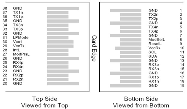

II. Pin Descriptions
|
Pin |
Symbol |
Name/Description |
Ref. |
|
1 |
GND |
Ground |
1 |
|
2 |
Tx2n |
Transmitter Inverted Data Input |
|
|
3 |
Tx2p |
Transmitter Non-Inverted Data Input |
|
|
4 |
GND |
Ground |
1 |
|
5 |
Tx4n |
Transmitter Inverted Data Input |
|
|
6 |
Tx4p |
Transmitter Non-Inverted Data Input |
|
|
7 |
GND |
Ground |
1 |
|
8 |
ModSe1L |
Module Select |
|
|
9 |
ResetL |
Module Reset |
|
|
10 |
Vcc Rx |
+3.3V Power supply receiver |
|
|
11 |
SCL |
2-wire serial interface clock |
|
|
12 |
SDA |
2-wire serial interface data |
|
|
13 |
GND |
Ground |
1 |
|
14 |
Rx3p |
Receiver Non-Inverted Data Output |
|
|
15 |
Rx3n |
Receiver Inverted Data Output |
|
|
16 |
GND |
Ground |
1 |
|
17 |
Rx1p |
Receiver Non-Inverted Data Output |
|
|
18 |
Rx1n |
Receiver Inverted Data Output |
|
|
19 |
GND |
Ground |
1 |
|
20 |
GND |
Ground |
1 |
|
21 |
Rx2n |
Receiver Inverted Data Output |
|
|
22 |
Rx2p |
Receiver Non-Inverted Data Output |
|
|
23 |
GND |
Ground |
1 |
|
24 |
Rx4n |
Receiver Inverted Data Output |
|
|
25 |
Rx4p |
Receiver Non-Inverted Data Output |
|
|
26 |
GND |
Ground |
1 |
|
27 |
ModPrSL |
Module Present |
|
|
28 |
IntL |
Interrupt |
|
|
29 |
Vcc Tx |
+3.3V Power supply transmitter |
|
|
30 |
Vcc1 |
+3.3V Power Supply |
|
|
31 |
LPMode |
Low Power Mode |
|
|
32 |
GND |
Ground |
1 |
|
33 |
Tx3p |
Transmitter Non-Inverted Data Input |
|
|
34 |
Tx3n |
Transmitter Inverted Data Input |
|
|
35 |
GND |
Ground |
1 |
|
36 |
Tx1p |
Transmitter Non-Inverted Data Input |
|
|
37 |
Tx1n |
Transmitter Inverted Data Input |
|
|
38 |
GND |
Ground |
1 |
Note:
1. Circuit ground is internally isolated from chassis ground.
III. Absolute Maximum Ratings
|
Parameter |
Symbol |
Min. |
Typ. |
Max. |
Unit |
Ref. |
|
Storage Temperature |
TS |
-40 |
|
85 |
ºC |
|
|
Storage Ambient Humidity |
HA |
5 |
|
95 |
% |
|
|
Maximum Supply Voltage |
VCC |
-0.5 |
|
3.6 |
V |
|
|
Lead Soldering Temperature/Time |
TSOLD |
|
|
260/10 |
ºC/sec |
1 |
|
Lead Soldering Temperature/Time |
TSOLD |
|
|
360/10 |
ºC/sec |
2 |
Note:
1.Suitable for wave soldering.
2. Only for soldering by iron.
IV. Optical Characteristics
|
Parameter |
Symbol |
Min. |
Typ. |
Max. |
Unit |
Ref. |
|
Transmitter(per lane) |
||||||
|
Signaling Speed per Lane |
|
25.78125 ± 100 ppm |
Gb/s |
1 |
||
|
Center Wavelength |
λC |
-- |
1264.5 – 1277.5 1284.5 – 1297.5 1304.5 – 1317.5 1324.5 – 1337.5 |
-- |
nm |
|
|
Extinction ratio |
ER |
3.5 |
-- |
-- |
dB |
|
|
Side Mode Suppression Ratio |
SMSR |
30 |
-- |
-- |
dB |
|
|
Total average launch power |
Ptot |
-- |
-- |
8.5 |
dBm |
|
|
Average launch power, each lane |
Po |
-6.5 |
-- |
2.5 |
dBm |
|
|
OMA, each lane |
OMA |
-4 |
-- |
2.5 |
dBm |
CW,ER>3.5dB |
|
Difference in launch power between any two lanes (OMA) |
|
|
|
5 |
dB |
|
|
TDP, each lane |
TDP |
|
|
3.0 |
dB |
2 |
|
Average launch power of OFF transmitter, each lane |
Poff |
|
|
-30 |
dBm |
|
|
Transmitter eye mask definition {X1,X2,X3,Y1,Y2,Y3} |
|
{0.31, 0.40, 0.45, 0.34, 0.38, 0.4} |
|
3 |
||
|
Receiver(per lane) |
||||||
|
Signaling Speed per Lane |
|
25.78125 ± 100 ppm |
Gb/s |
4 |
||
|
Input Optical Wavelength |
λin |
|
1264.5 – 1277.5 1284.5 – 1297.5 1304.5 – 1317.5 1324.5 – 1337.5 |
|
nm |
|
|
Damage threshold |
|
3.5 |
|
|
dBm |
|
|
Receiver Power (OMA), each Lane |
|
2.5 |
|
|
dBm |
|
|
Rx Sensitivity(OMA) per lane |
RSENS |
|
|
-10 |
dBm |
5 |
|
Stressed receiver sensitivity (OMA), each lane |
SRS |
|
|
-7.3 |
dBm |
6 |
|
Conditions of stressed receiver sensitivity test: |
||||||
|
Vertical eye closure penalty, each lane |
VECP |
1.9 |
|
dB |
|
|
|
Stressed eye J2 jitter, each lane |
J2 |
0.33 |
|
UI |
|
|
|
Stressed eye J4 jitter, each lane |
J4 |
0.48 |
|
UI |
|
|
|
SRS eye mask definition {X1, X2, X3, Y1, Y2, Y3} |
|
{0.39, 0.50, 0.50, 0.39, 0.39, 0.4} |
|
|
||
|
Loss of Signal Assert |
PA |
-30 |
|
- |
dBm |
|
|
Loss of Signal De-assert |
PD |
|
|
-11. |
dBm |
|
|
LOS Hysteresis |
PD - PA |
0.5 |
|
|
dB |
|
Note :
1. Transmitter consists of 4 lasers operating at 25.78Gb/s each.
2. TDP value does not include MPI penalty.
3. Hit ratio of 5x10⁻⁵, per IEEE.
4. Receiver consists of 4 photodetectors operating at 25.78Gb/s each.
5.Sensitivity is specified at 5x10⁻⁵ BER.
6.Measured with CWDM4 MSA2 conformance test signal at TP3 for 5x10⁻⁵ BER.
V. Digital Diagnostic Functions
ESBQLC23-K02C QSFP28 transceivers support the I2C-based diagnostics interface specified by the QSFP28 MSA.
VI. Electrical Interface Characteristics
|
Parameter |
Symbol |
Min. |
Typ. |
Max. |
Unit |
Ref. |
||
|
Supply Voltage |
VCC |
3.135 |
|
3.465 |
V |
|
||
|
Supply Current |
ICC |
|
|
1.12 |
A |
|
||
|
Module total power |
P |
|
|
3.5 |
W |
1 |
||
|
Transmitter |
||||||||
|
Signaling rate per lane |
|
25.78125±100ppm |
Gb/s |
|
||||
|
Differential data input swing per lane |
Vin,pp |
900 |
|
|
mV |
|
||
|
Differential input return loss(min) |
RLd(f) |
9.5 – 0.37f, 0.01≤f<8 4.75-7.4log10(f/14), 8≤f<19 |
dB |
|
||||
|
Differential to common mode input return loss(min) |
RLdc(f) |
22-20(f/25.78), 0.01≤f<12.89 15-6(f/25.78), 12.89≤f<19 |
dB |
|
||||
|
Differential termination mismatch |
|
|
|
10 |
% |
|
||
|
Eye width |
|
|
0.46 |
|
UI |
|
||
|
Applied pk-pk sinusoidal Jitter |
|
Per IEEE802.3bm Table 88-13 |
|
|
||||
|
Eye height |
|
|
95 |
|
mV |
|
||
|
Receiver |
||||||||
|
Signaling rate per lane |
|
25.78125±100ppm |
Gb/s |
|
||||
|
Differential data output swing |
Vout,pp |
100 |
|
400 |
mVpp |
2 |
||
|
300 |
|
600 |
||||||
|
400 |
600 |
800 |
||||||
|
600 |
|
1200 |
||||||
|
Eye width |
|
0.57 |
|
|
UI |
|
||
|
Vertical eye closure |
VEC |
|
|
5.5 |
dB |
|
||
|
Differential output return loss (min) |
RLd(f) |
9.5 – 0.37f, 0.01≤f<8 4.75 – 7.4log10(f/14), 8 ≤f<19 |
dB |
|
||||
|
Common to differential mode conversion return loss (min) |
RLdc(f) |
22-20(f/25.78), 0.01≤f<12.89 15-6(f/25.78), 12.89≤f<19 |
dB |
|
||||
|
Differential termination mismatch |
|
|
|
10 |
% |
|
||
Note :
1.Maximum total power value is specified across the full temperature and voltage range.
2.Output voltage is settable in 4 discrete range via I2C.Default range is Range 2 ( 400 – 800mV ).
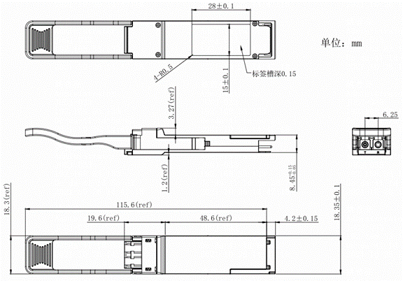
VII. Mechanical Specifications (Unit: mm)
Want to know about this product?
If you are interested in our products and want to know more details,please leave a message here,we will reply you as soon as we can.
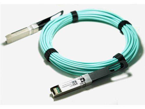 LPQQAA31-M(L)xxC
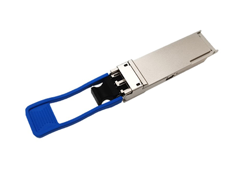 LPBQLB31-K10C
 LPBQCM85-S10C

Address : East of 2F, Tianmen Optical Valley Science Park,Qiaoxiang Economic development area,Tianmen, Hubei Province.
Tel : 15012662571
Email : chris.peng@talptech.com
Skype : 15012662571