APPLICATIONS
l 100GBASE-LR4 100G Ethernet
Compliance
l QSFP28 MSA.
l IEEE802.3bm and IEEE802.3ba
l SFF-8636
l RoHS
Ordering information
|
Part No. |
Bit Rate (Gbps) |
Laser (nm) |
Distance |
Fiber Type |
DDMI |
Connector |
Temp |
|
ESBQLB31-K10C |
4*25.78125 |
LWDM |
10km |
SMF |
YES |
LC |
0℃~+70℃ |
I. Pin Diagram
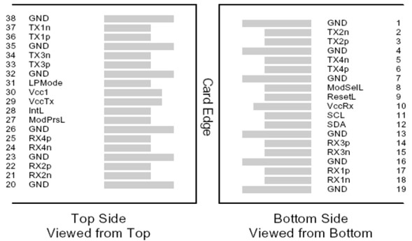

II. Pin Descriptions
|
Pin |
Symbol |
Name/Description |
Ref. |
|
1 |
GND |
Ground |
1 |
|
2 |
Tx2n |
Transmitter Inverted Data Input |
|
|
3 |
Tx2p |
Transmitter Non-Inverted Data Input |
|
|
4 |
GND |
Ground |
1 |
|
5 |
Tx4n |
Transmitter Inverted Data Input |
|
|
6 |
Tx4p |
Transmitter Non-Inverted Data Input |
|
|
7 |
GND |
Ground |
1 |
|
8 |
ModSe1L |
Module Select |
|
|
9 |
ResetL |
Module Reset |
|
|
10 |
Vcc Rx |
+3.3V Power supply receiver |
|
|
11 |
SCL |
2-wire serial interface clock |
|
|
12 |
SDA |
2-wire serial interface data |
|
|
13 |
GND |
Ground |
1 |
|
14 |
Rx3p |
Receiver Non-Inverted Data Output |
|
|
15 |
Rx3n |
Receiver Inverted Data Output |
|
|
16 |
GND |
Ground |
1 |
|
17 |
Rx1p |
Receiver Non-Inverted Data Output |
|
|
18 |
Rx1n |
Receiver Inverted Data Output |
|
|
19 |
GND |
Ground |
1 |
|
20 |
GND |
Ground |
1 |
|
21 |
Rx2n |
Receiver Inverted Data Output |
|
|
22 |
Rx2p |
Receiver Non-Inverted Data Output |
|
|
23 |
GND |
Ground |
1 |
|
24 |
Rx4n |
Receiver Inverted Data Output |
|
|
25 |
Rx4p |
Receiver Non-Inverted Data Output |
|
|
26 |
GND |
Ground |
1 |
|
27 |
ModPrSL |
Module Present |
|
|
28 |
IntL |
Interrupt |
|
|
29 |
Vcc Tx |
+3.3V Power supply transmitter |
|
|
30 |
Vcc1 |
+3.3V Power Supply |
|
|
31 |
LPMode |
Low Power Mode |
|
|
32 |
GND |
Ground |
1 |
|
33 |
Tx3p |
Transmitter Non-Inverted Data Input |
|
|
34 |
Tx3n |
Transmitter Inverted Data Input |
|
|
35 |
GND |
Ground |
1 |
|
36 |
Tx1p |
Transmitter Non-Inverted Data Input |
|
|
37 |
Tx1n |
Transmitter Inverted Data Input |
|
|
38 |
GND |
Ground |
1 |
Note:
1. Circuit ground is internally isolated from chassis ground.
III. Absolute Maximum Ratings
|
Parameter |
Symbol |
Min. |
Typ. |
Max. |
Unit |
Ref. |
|
Storage Temperature |
TS |
-40 |
|
85 |
ºC |
|
|
Storage Ambient Humidity |
HA |
5 |
|
95 |
% |
|
|
Maximum Supply Voltage |
VCC |
-0.5 |
|
4.0 |
V |
|
|
Signal Input Voltage |
|
-0.3 |
|
Vcc+0.3 |
V |
|
|
Receiver Damage Threshold |
|
+5.5 |
|
|
dBm |
|
|
Lead Soldering Temperature/Time |
TSOLD |
|
|
260/10 |
ºC/sec |
1 |
|
Lead Soldering Temperature/Time |
TSOLD |
|
|
360/10 |
ºC/sec |
2 |
Note:
1.Suitable for wave soldering.
2. Only for soldering by iron.
IV. General Product Characteristics
|
Parameter |
Symbol |
Min. |
Typ. |
Max. |
Unit |
Ref. |
|
Data Rate (per line) |
BR |
|
25.78125 |
|
Gbps |
|
|
Case Operating Temperature |
Tcase |
0 |
- |
70 |
ºC |
|
|
Power Supply Voltage |
Vcc |
3.13 |
3.3 |
3.47 |
V |
|
|
Transmission Distance |
TD |
|
- |
10 |
km |
|
|
Coupled fiber |
Single mode fiber |
9/125um SMF |
||||
V. Optical Characteristics
|
Parameter |
Symbol |
Min. |
Typ. |
Max. |
Unit |
Ref. |
|
Transmitter(per lane) |
||||||
|
Total Average Output Power |
POUT |
|
|
10.5 |
dBm |
|
|
Average Launch Power per lane |
TXPx |
-4.3 |
|
4.5 |
dBm |
|
|
Transmit OMA per Lane |
TxOMA |
-1.3 |
|
4.5 |
dBm |
|
|
Extinction Ratio |
ER |
4 |
|
|
dB |
|
|
Center Wavelength |
λC |
|
1299.02 ~ 1301.09 1303.54 ~ 1305.63 1308.09 ~ 1310.19 |
|
nm |
|
|
RMS Spectral Width |
σ |
|
|
1 |
nm |
|
|
Transmitter OFF Output Power |
POff |
|
|
-30 |
dBm |
|
|
Transmitter eye mask definition {X1,X2,X3,Y1,Y2,Y3} |
|
{0.25,0.4,0.45,0.25,0.28,0.4} |
|
1 |
||
|
Receiver(per lane) |
||||||
|
Input Optical Wavelength |
λIN |
|
1299.02 ~ 1301.09 1303.54 ~ 1305.63 1308.09 ~ 1310.19 |
|
nm |
|
|
Rx Sensitivity(OMA) per lane |
RSENS |
|
|
-8.6 |
dBm |
|
|
Input Saturation Power (Overload) |
PSAT |
|
|
+4.5 |
dBm |
|
|
Receiver Reflectance |
Rfl |
|
|
-26 |
dBm |
|
|
Loss of Signal Assert |
PA |
-30 |
|
|
dBm |
|
|
Loss of Signal De-assert |
PD |
|
|
-11 |
dBm |
|
|
LOS Hysteresis |
PD - PA |
0.5 |
|
|
dB |
|
Note:
1. Hit ratio 5x10⁻⁵.
VI. Digital Diagnostic Functions
ESBQLB31-K10C QSFP28 transceivers support the I2C-based diagnostics interface specified by the QSFP28 MSA.
VII. Electrical Interface Characteristics
|
Parameter |
Symbol |
Min. |
Type |
Max. |
Unit |
Ref. |
|
Transmitter |
||||||
|
Signaling rate (each lane) |
SR |
|
25.78125 |
|
Gbps |
|
|
Differential data input voltage per lane |
Vin,pp,diff |
- |
- |
900 |
mV |
|
|
Differential termination mismatch |
- |
- |
- |
10 |
% |
|
|
Single-ended voltage tolerance range |
- |
-0.4 |
- |
3.3 |
V |
|
|
DC common mode voltage |
- |
-350 |
- |
2850 |
mV |
|
|
Receiver |
||||||
|
Signaling rate (each lane) |
SR |
|
25.78125 |
|
Gbps |
|
|
Differential output voltage |
- |
- |
- |
900 |
mV |
|
|
Eye width |
- |
0.57 |
- |
- |
UI |
|
|
Eye height |
- |
228 |
- |
- |
mV |
|
|
Differential termination mismatch |
- |
|
- |
10 |
% |
|
|
Transition time (min, 20% to 80%) @LR4 |
- |
12 |
- |
- |
ps |
|
|
Transition time (min, 20% to 80%) @OTU4 |
- |
9.5 |
- |
- |
ps |
|
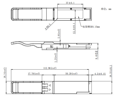
VIII.Mechanical Specifications (Unit: mm)
compatible with SFF-8661.
Want to know about this product?
If you are interested in our products and want to know more details,please leave a message here,we will reply you as soon as we can.
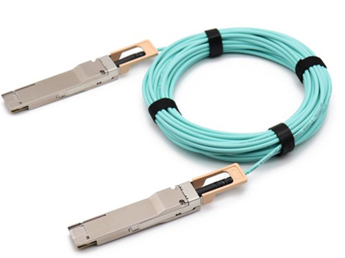
 LPQQAA31-M(L)xxC
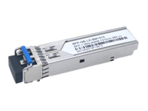
 LPBQLC23-K02C
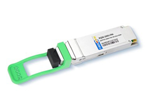
 LPBQCM85-S10C

Address : East of 2F, Tianmen Optical Valley Science Park,Qiaoxiang Economic development area,Tianmen, Hubei Province.
Tel : 15012662571
Email : chris.peng@talptech.com
Skype : 15012662571