APPLICATIONS
l 50GBASE-ER
l Other Optical Link
Compliance
l SFF-8431.
l IEEE802.3cd
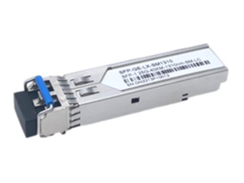
l SFP56 MSA
l RoHS
Ordering information
|
Part No. |
Bit Rate (Gbps) |
Laser (nm) |
Distance |
Fiber Type |
DDMI |
Connector |
Temp |
|
ESZPLE23-K40C |
53.125 |
1270 |
40km |
SMF |
YES |
LC |
0℃~+70℃ |
|
ESZPLE32-K40C |
53.125 |
1313 |
40km |
SMF |
YES |
LC |
0℃~+70℃ |
|
ESZPLE23-K40I |
53.125 |
1270 |
40km |
SMF |
YES |
LC |
-40℃~+85℃ |
|
ESZPLE32-K40I |
53.125 |
1313 |
40km |
SMF |
YES |
LC |
-40℃~+85℃ |
I. Pin Diagram
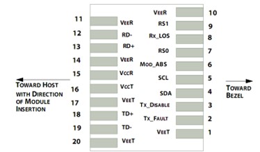
Pin out of Connector Block on Host Board
II. Pin Descriptions
|
Pin |
Symbol |
Name/Description |
Ref. |
|
1 |
VEET |
Transmitter Ground (Common with Receiver Ground) |
1 |
|
2 |
TFAULT |
Transmitter Fault. |
2 |
|
3 |
TDIS |
Transmitter Disable. Laser output disabled on high or open. |
3 |
|
4 |
SDA |
2-wire Serial Interface Data Line |
4 |
|
5 |
SCL |
2-wire Serial Interface Clock Line |
4 |
|
6 |
MOD_ABS |
Module Absent. Grounded within the module |
4 |
|
7 |
RS0 |
Rate Select 0 |
6 |
|
8 |
LOS |
Loss of Signal indication. Logic “0” indicates normal operation. |
5 |
|
9 |
RS1 |
Rate select 1 |
6 |
|
10 |
VEER |
Receiver Ground (Common with Transmitter Ground) |
1 |
|
11 |
VEER |
Receiver Ground (Common with Transmitter Ground) |
1 |
|
12 |
RD- |
Receiver Inverted DATA out. AC Coupled |
|
|
13 |
RD+ |
Receiver Non-inverted DATA out. AC Coupled |
|
|
14 |
VEER |
Receiver Ground (Common with Transmitter Ground) |
1 |
|
15 |
VCCR |
Receiver Power Supply |
|
|
16 |
VCCT |
Transmitter Power Supply |
|
|
17 |
VEET |
Transmitter Ground (Common with Receiver Ground) |
1 |
|
18 |
TD+ |
Transmitter Non-Inverted DATA in. AC Coupled. |
|
|
19 |
TD- |
Transmitter Inverted DATA in. AC Coupled. |
|
|
20 |
VEET |
Transmitter Ground (Common with Receiver Ground) |
1 |
Notes:
1. Circuit ground is internally isolated from chassis ground.
2. TFAULT is an open collector/drain output, which is pulled up with a 4.7kΩ – 10kΩ resistor on the host board if intended for use. Pull up voltage should be between 2.0V to Vcc + 0.3V. A high output indicates a transmitter fault caused by either the TX bias current or the TX output power exceeding the preset alarm threshold. A low output indicates normal operation. In the low state, the output is pulled to <0.8V.
3. Laser output disabled on TDIS >2.0V or open, enabled on TDIS <0.8V.
4. Should be pulled up with 4.7kΩ – 10kΩ on host board to a voltage between 2.0V and 3.6V. MOD_ABS pulls line low to indicate module is plugged in.
5. LOS is open collector output. Should be pulled up with 4.7kΩ – 10kΩ on host board to a voltage between 2.0V and 3.6V. Logic 0 indicates normal operation; logic 1 indicates loss of signal.
6. Internally pulled down per SFF-8431 Rev 4.1.
III. Absolute Maximum Ratings
|
Parameter |
Symbol |
Min. |
Typ. |
Max. |
Unit |
Ref. |
|
Maximum Supply Voltage |
Vcc |
-0.5 |
|
3.6 |
V |
|
|
Storage Temperature |
TS |
-40 |
|
85 |
℃ |
|
|
Relative Humidity |
RH |
5 |
|
85 |
% |
|
IV. Optical Characteristics
|
Parameter |
Symbol |
Min. |
Typ. |
Max. |
Unit |
Remark |
|
Transmitter |
||||||
|
Center Wavelength |
λc |
|
1270 |
|
nm |
ESZPLE23-K40C(I) |
|
|
1313 |
|
nm |
ESZPLE32-K40C(I) |
||
|
Spectral Width(-20dB) |
Pm |
|
|
1 |
nm |
|
|
Average Output Power |
Pavg |
0.6 |
|
6.6 |
dBm |
|
|
Optical Modulation Amplitude(OMA outer) |
OMA |
3.4 |
|
7.4 |
|
|
|
Extinction Ratio |
ER |
6 |
|
|
dB |
|
|
Transmitter and dispersion eye closure(TDEC) |
TDEC |
|
|
3.2 |
dB |
|
|
Side Mode Suppression Ratio |
SMSR |
30 |
|
|
dB |
|
|
Transmitter OFF Output Power |
POff |
|
|
-30 |
dBm |
|
|
Receiver |
||||||
|
Center Wavelength |
λc |
|
1313 |
|
nm |
ESZPLE32-K40C(I) |
|
|
1270 |
|
nm |
ESZPLE23-K40C(I) |
||
|
Receiver Sensitivity(OMA) |
RSENSE |
|
-17 |
-15.1 |
dBm |
1 |
|
Averge receive power |
Pin |
-17.6 |
|
-3.4 |
dBm |
|
|
Receiver Reflectance |
Rfl |
|
|
-26 |
dBm |
|
|
Loss of Signal Assert |
PA |
-25 |
|
|
dBm |
|
|
Loss of Signal De-assert |
PD |
|
|
-18 |
dBm |
|
|
LOS Hysteresis |
PD- PA |
0.5 |
|
|
dB |
|
Note:
1. Measured with conformance test signal at TP3 for BER =2.4E-4 Pre-FEC.
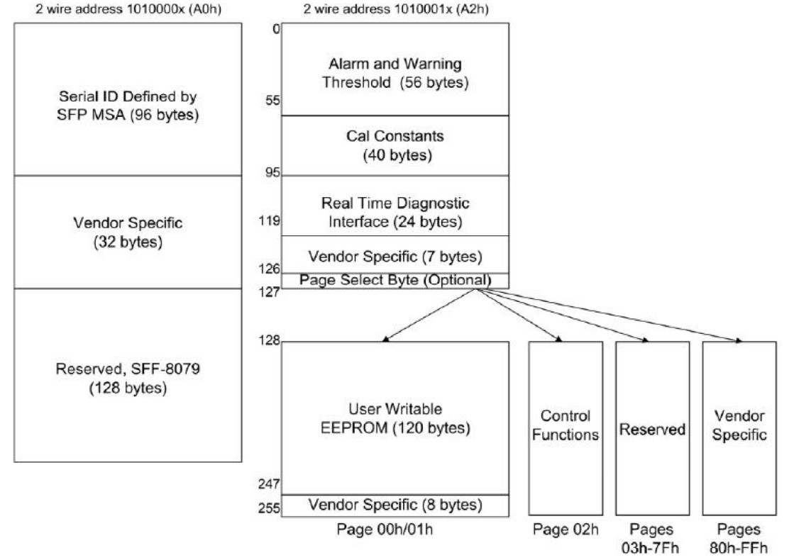
V. Digital Diagnostic Memory Map
VI. Digital Diagnostic Specifications
|
Parameter |
Unit |
Accuracy |
|
Case Temperature |
℃ |
±3 |
|
Supply Voltage |
V |
±3% |
|
Tx Bias Current |
mA |
±10% |
|
Tx Optical Power |
dB |
±3 |
|
Rx Optical Power |
dB |
±3 |
VII. Electrical Interface Characteristics
|
Parameter |
Symbol |
Min |
Type |
Max |
Unit |
Ref. |
|
Supply Voltage |
Vcc |
3.135 |
3.3 |
3.465 |
V |
|
|
Power dissipation |
Pd |
|
|
3 |
W |
|
|
Bite rate |
BR |
|
53.125 |
|
Gb/s |
|
|
Input differential impedance |
Rin |
|
100 |
|
|
1 |
|
Differential data input swing |
Vin, pp |
|
|
900 |
mV |
|
|
Input Logic Level Hig |
VIH |
2 |
|
VccHOST |
V |
|
|
Input Logic Level Low |
VIL |
Vee |
|
Vee+0.8 |
V |
|
|
Output Logic Level High |
VOH |
VccHOST-0.5 |
|
VccHOST |
V |
|
|
Output Logic Level Low |
VOL |
Vee |
|
Vee+0.4 |
V |
|
Notes:
1. Differential voltage amplitude is measured between TxnP / TxnN/ TxnP / TxnN.
2.
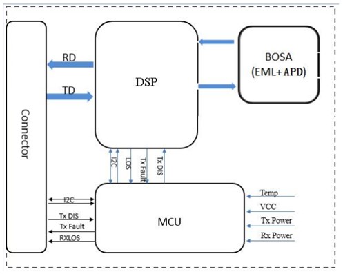
VIII.Recommended Interface Circuit
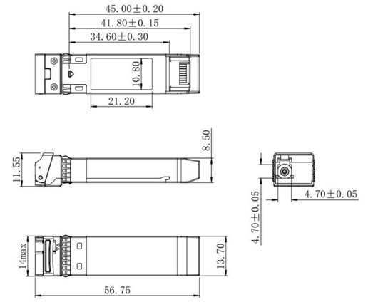
IX. Mechanical Specifications (Unit: mm)
Want to know about this product?
If you are interested in our products and want to know more details,please leave a message here,we will reply you as soon as we can.

Address : East of 2F, Tianmen Optical Valley Science Park,Qiaoxiang Economic development area,Tianmen, Hubei Province.
Tel : 15012662571
Email : chris.peng@talptech.com
Skype : 15012662571