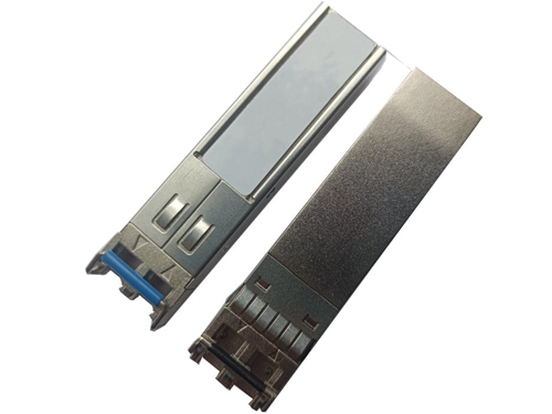
APPLICATIONS
l 800GBASE-SR8 800G Ethernet
l Data center
Compliance
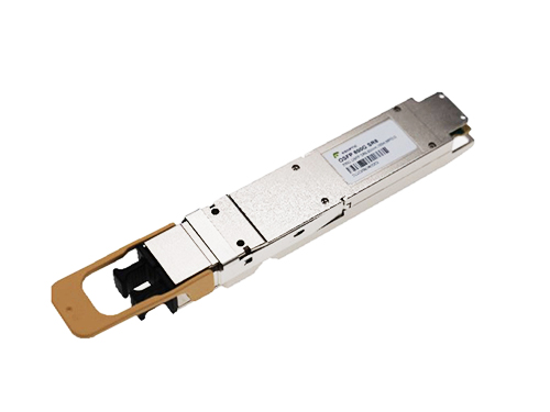
l OSFP MSA.
l IEEE802.3ck
l RoHS
Ordering information
|
Part NO. |
Bit Rate (Gbps) |
Laser (nm) |
Distance(m) |
Media |
DDMI |
Connector |
Temp(℃) |
|
ESXWMM85-S10C |
425 |
850 |
100 (OM4) |
multi-mode fiber |
YES |
MPO-16(APC) |
0~70 |
|
ESXWHM85-S10C |
425 |
850 |
100 (OM4) |
multi-mode fiber |
YES |
2XMPO-12(APC) |
0~70 |
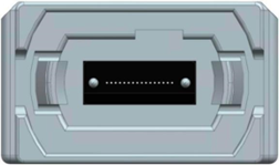
I. Pin Diagram
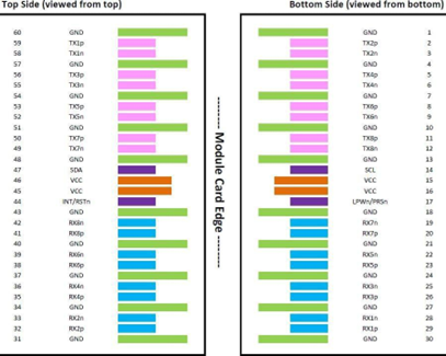
Figure 1
II. Pin Descriptions
|
Pin |
Name |
Logic |
Description |
Plug Sequence |
Notes |
|
1 |
GND |
|
Ground |
1 |
|
|
2 |
Tx2p |
CML-I |
Receiver Data Non-Inverted |
3 |
|
|
3 |
Tx2n |
CML-I |
Receiver Data Inverted |
3 |
|
|
4 |
GND |
|
Ground |
1 |
|
|
5 |
Tx4p |
CML-I |
Receiver Data Non-Inverted |
3 |
|
|
6 |
Tx4n |
CML-I |
Receiver Data Inverted |
3 |
|
|
7 |
GND |
|
Ground |
1 |
|
|
Pin |
Name |
Logic |
Description |
Plug Sequence |
Notes |
|
8 |
Tx6p |
CML-I |
Receiver Data Non-Inverted |
3 |
|
|
9 |
Tx6n |
CML-I |
Receiver Data Inverted |
3 |
|
|
10 |
GND |
|
Ground |
1 |
|
|
11 |
TX8p |
CML-I |
Receiver Data Non-Inverted |
3 |
|
|
12 |
TX8n |
CML-I |
Receiver Data Inverted |
3 |
|
|
13 |
GND |
|
Ground |
1 |
|
|
14 |
SCL |
LVCMOS- I/O |
2-wire Serial interface clock |
3 |
|
|
15 |
VCC |
|
+3.3V Power |
2 |
|
|
16 |
VCC |
|
+3.3V Power |
2 |
|
|
17 |
LPWn/PRSn |
Multi- Level |
Low-Power Mode / Module Present |
3 |
|
|
18 |
GND |
|
Ground |
1 |
|
|
19 |
RX7n |
CML-O |
Receiver Data Inverted |
3 |
|
|
20 |
RX7p |
CML-O |
Receiver Data Non-Inverted |
3 |
|
|
21 |
GND |
|
Ground |
1 |
|
|
22 |
RX5n |
CML-O |
Receiver Data Inverted |
3 |
|
|
23 |
RX5p |
CML-O |
Receiver Data Non-Inverted |
3 |
|
|
24 |
GND |
|
Ground |
1 |
|
|
25 |
RX3n |
CML-O |
Receiver Data Inverted |
3 |
|
|
26 |
RX3p |
CML-O |
Receiver Data Non-Inverted |
3 |
|
|
27 |
GND |
|
Ground |
1 |
|
|
28 |
RX1n |
CML-O |
Receiver Data Inverted |
3 |
|
|
29 |
RX1p |
CML-O |
Receiver Data Non-Inverted |
3 |
|
|
30 |
GND |
|
Ground |
1 |
|
|
31 |
GND |
|
Ground |
1 |
|
|
32 |
RX2p |
CML-O |
Receiver Data Non-Inverted |
3 |
|
|
33 |
RX2n |
CML-O |
Receiver Data Inverted |
3 |
|
|
34 |
GND |
|
Ground |
1 |
|
|
35 |
RX4p |
CML-O |
Receiver Data Non-Inverted |
3 |
|
|
Pin |
Name |
Logic |
Description |
Plug Sequence |
Notes |
|
36 |
RX4n |
CML-O |
Receiver Data Inverted |
3 |
|
|
37 |
GND |
|
Ground |
1 |
|
|
38 |
RX6p |
CML-O |
Receiver Data Non-Inverted |
3 |
|
|
39 |
RX6n |
CML-O |
Receiver Data Inverted |
3 |
|
|
40 |
GND |
|
Ground |
1 |
|
|
41 |
RX8p |
CML-O |
Receiver Data Non-Inverted |
3 |
|
|
42 |
RX8n |
CML-O |
Receiver Data Inverted |
3 |
|
|
43 |
GND |
|
Ground |
1 |
|
|
44 |
INT/RSTn |
Multi- Level |
Module Interrupt / Module Reset |
3 |
1B |
|
45 |
VCC |
|
+3.3V Power |
2 |
|
|
46 |
VCC |
|
+3.3V Power |
2 |
|
|
47 |
SDA |
LVCMOS- I/O |
2-wire Serial interface data |
3 |
|
|
48 |
GND |
|
Ground |
1 |
|
|
49 |
TX7n |
CML-I |
Transmitter Data Inverted |
3 |
|
|
50 |
TX7p |
CML-I |
Transmitter Data Non-Inverted |
3 |
|
|
51 |
GND |
|
Ground |
1 |
|
|
52 |
TX5n |
CML-I |
Transmitter Data Inverted |
3 |
|
|
53 |
TX5p |
CML-I |
Transmitter Data Non-Inverted |
3 |
|
|
54 |
GND |
|
Ground |
1 |
|
|
55 |
TX3n |
CML-I |
Transmitter Data Inverted |
3 |
|
|
56 |
TX3p |
CML-I |
Transmitter Data Non-Inverted |
3 |
|
|
57 |
GND |
|
Ground |
1 |
|
|
58 |
TX1n |
CML-I |
Transmitter Data Inverted |
3 |
|
|
59 |
TX1p |
CML-I |
Transmitter Data Non-Inverted |
3 |
|
|
60 |
GND |
|
Ground |
1 |
|
Notes:
1. Plug Sequence specifies the mating sequence of the host connector and module. The contact sequence is 1,2,3.
2. LPWn/PRSn is a Multi-level signal for low power control from host to module and module presence indication from module to host. It designed according to OSFP Module Specification Section 13.5.3
3. INT/RSTn is a Multi-level signal for interrupt request from module to host and reset control from host to module. It designed according to OSFP Module Specification Section 13.5.2.
III. Absolute Maximum Ratings
|
Parameter |
Symbol |
Min. |
Typ. |
Max. |
Unit |
Ref. |
|
Storage Temperature |
TS |
-40 |
|
85 |
ºC |
|
|
Storage Ambient Humidity |
HA |
15 |
|
85 |
% |
|
|
Maximum Supply Voltage |
VCC |
-0.5 |
|
3.6 |
V |
|
|
Receiver damage Threshold,per lane |
|
5 |
|
|
dBm |
|
|
Lead Soldering Temperature/Time |
TSOLD |
|
|
260/10 |
ºC/sec |
Note1 |
|
Lead Soldering Temperature/Time |
TSOLD |
|
|
360/10 |
ºC/sec |
Note2 |
Notes:
1. Suitable for wave soldering.
2. Only for soldering by iron.
IV. Recommended Operating Conditions
|
Data Rate Spcifications |
Symbol |
Min. |
Typ. |
Max. |
Unit |
Ref. |
|
Supply Voltage |
Vcc |
3.135 |
3.3 |
3.465 |
V |
|
|
Supply Voltage Noise Tolerance |
PSNR |
|
|
66 |
mV |
10Hz~10MHz |
|
Instantaneous peak current at high power enable |
Icc_ip |
|
|
5600 |
mA |
|
|
Sustained peak current at high power enable |
Icc_sp |
|
|
4666 |
mA |
|
|
Supply steady state Current |
Icc |
|
|
4466 |
mA |
Steady state |
|
Operating Case Temperature |
Tc |
0 |
|
70 |
℃ |
|
|
Link distance on OM4 MMF |
d |
|
|
100 |
meters |
|
V. Optical Characteristics
|
Parameter |
Symbol |
Min. |
Typ. |
Max. |
Unit |
Ref. |
||
|
Transmitter(per lane) |
||||||||
|
Channel data rate |
fDC |
106.25 |
Gb/s |
|
||||
|
Signaling rate |
FSG |
53.125 |
GBd |
PAM4 |
||||
|
Signal speed variation from nominal |
⊿fSG |
-100 |
|
+100 |
Ppm |
|
||
|
Center Wavelength |
λC |
840 |
|
860 |
nm |
|
||
|
RMS Spectral Width |
σ |
|
|
0.6 |
nm |
Note1 |
||
|
Average Launch power ,each lane |
|
-4.6 |
|
4 |
dBm |
|
||
|
Outer Optical Modulation Amplitude (OMAouter), each lane |
max(TECQ, TDECQ) ≤ 1.8dB |
|
-2.6 |
|
3.5 |
dBm |
|
|
|
1.8 < max (TECQ, TDECQ) ≤ 4.4dB |
-4.4 + max(TE CQ, TDECQ) |
|||||||
|
Transmitter and dispersion eye closure for PAM4, each lane |
TDECQ |
|
|
4.4 |
dB |
|
||
|
Transmitter eye closure for PAM4 (TECQ), each lane |
TECQ |
|
|
4.4 |
|
|
||
|
Transmitter power excursion, each lane |
|
|
|
2.3 |
|
|
||
|
Average Optical Output Power of Off Transmitter, each lane |
Poff |
|
|
-30 |
dBm |
|
||
|
Extinction Ratio, each lane |
ER |
2.5 |
|
|
dB |
|
||
|
Optical return loss tolerance |
|
|
|
14 |
dB |
|
||
|
Encircled flux |
|
≥86% at 19um ≤30% at 45um |
|
Note 2 |
||||
|
Receiver(per lane) |
||||||||
|
Damage threshold |
|
5 |
|
|
dBm |
Note 3 |
||
|
Average receive power, each lane |
|
–6.4 |
|
4.0 |
dBm |
Note 4 |
||
|
Receive power (OMAouter), each lane |
|
|
|
3.5 |
dBm |
|
||
|
Receiver reflectance |
|
|
|
-15 |
dB |
|
||
|
Receiver sensitivity(OMA outer), each lane |
TECQ ≤ 1.8dB |
|
|
|
-4.6 |
dBm |
Note 5 Figure 2 |
|
|
1.8 < TECQ ≤ 4.4dB |
-6.4+ TECQ |
|||||||
|
Receiver Loss of Signal Indicator Assert Level |
LOSA |
-15 |
|
|
dBm |
|
||
|
Receiver Loss of Signal Indicator De-assert Level |
LOSD |
|
|
-7.5 |
dBm |
|
||
|
Hysteresis |
LOSH |
0.5 |
|
5 |
dB |
|
||
|
Stressed receiver sensitivity (OMAouter), each lane |
|
|
|
-2 |
dBm |
Note 5, 6 |
||
|
Conditions of stressed receiver sensitivity test: |
Note 7 |
|||||||
|
Stressed eye closure for PAM4(SECQ), lane under test |
4.4 |
dB |
|
|||||
|
OMAouter of each aggressor lane |
3.5 |
dBm |
|
|||||
Notes:
1. RMS spectral width is the standard deviation of the spectrum
2. If measured into type A1a.2 or type A1a.3, or A1a.4, 50 um fiber, in accordance with IEC 61280-1-4.
3. The receiver shall be able to tolerate, without damage, continuous exposure to an optical input signal having this average power level on one lane. The receiver does not have to operate correctly at this input power.
4. Average receive power, each lane (min) is not the principal indicator of signal strength. A received power below this value cannot be compliant; however, a value above this does not ensure compliance.
5. For when Pre-FEC BER is 2.4 x 10⁻⁴.
6. Measured with conformance test signal at TP3 (see 167.8.14) for the BER specified in 167.1.1.
7. These test conditions are for measuring stressed receiver sensitivity. They are not characteristics of the receiver.
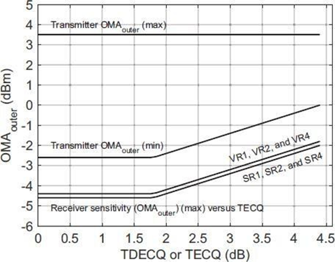
Figure 2 Receiver Sensitivity
VI. Electrical Interface Characteristics
|
Parameter |
Symbol |
Min. |
Typ. |
Max. |
Unit |
Ref. |
|
Supply Voltage |
VCC |
3.135 |
|
3.465 |
V |
|
|
Power Dissipation |
Pd |
|
|
14 |
W |
|
|
Transmitter(per Lane) |
||||||
|
Signaling rate per lane (range) |
|
-100ppm |
53.125 |
+100ppm |
GBd |
PAM4 |
|
Differential data output swing |
|
300 |
|
900 |
mVpp |
|
|
Eye height |
|
15 |
|
|
mV |
|
|
Vertical eye closure [VEC] |
|
|
|
12 |
dB |
|
|
Common-mode to differential-mode return loss [RLdc] |
|
Equation (120G-1) |
|
|
dB |
Note 2 |
|
Effective return loss [ERL] |
|
8.5 |
|
|
dB |
|
|
Differential termination mismatch |
|
|
|
10 |
% |
|
|
Transition time (20% to 80%) |
|
8.5 |
|
|
ps |
|
|
Receiver (per Lane) |
||||||
|
Signaling rate, each lane (range) |
|
-100ppm |
53.125 |
+100ppm |
GBd |
at TP1 |
|
Differential pk-pk input voltage tolerance |
|
750 |
|
|
mV |
at TP1a |
|
Differential-mode to common-mode return loss [RLcd] |
|
Equation (120G-1) |
|
|
dB |
at TP1, Note 2 |
|
Effective return loss [ERL] |
|
7.3 |
|
|
dB |
at TP1 |
|
Differential termination mismatch |
|
|
|
10 |
% |
at TP1 |
|
Vertical eye closure |
|
|
|
12 |
dB |
at TP1 |
|
Transition Time |
|
10 |
|
|
ps |
at TP1 |
Notes:
1. Electrical module output is squelched for loss of optical input signal.
2. IEEE P802.3ck D3p0 [1]
Figure 3
VII. HIGH SPEED DATAINTERFACE
Rx(n)(p/n)
Rx(n)(p/n) are OSFP module receiver data outputs. Rx(n)(p/n) are AC-coupled 100 Ohm differential lines that should be terminated with 100 Ohm differentially at the Host ASIC(SerDes). The AC coupling is inside the OSFP module and not required on the Host board. When properly terminated, the differential voltage swing shall be less than or equal to 900 mVpp or as defined by the relevant standard, or whichever is less. Output squelch for loss of optical input signal, hereafter Rx Squelch, is required and shall function as follows. In the event of the Rx input signal on any optical port becoming equal to or less than the level required to assert LOS, then the receiver output(s) associated with that Rx port shall be squelched. A single Rx optical port can be associated with more than one Rx output. In the squelched state output impedance levels are maintained while the differential voltage amplitude shall be less than 50 mVpp.
In module operation, default Rx auto squelch is enable. But Rx auto squelch and force squelching function are not supported.
Tx(n)(p/n)
Tx(n)(p/n) are OSFP module transmitter data inputs. They are AC-coupled 100 Ohm differential lines with 100 Ohm differential terminations inside the OSFP optical module. TheAC coupling is implemented inside the OSFP optical module and not required on the Host board.
Output squelch for loss of electrical signal, hereafter Tx Squelch, is an optional function. Where implemented it shall function as follows. In the event of the differential, peak-to-peak electrical signal amplitude on any electrical input lane becoming less than 70 mVpp, then the transmitter optical output associated with that electrical input lane shall be squelched and the associated TxLOS flag set. If multiple electrical input lanes are associated with the same optical output lane, the loss of any of the incoming electrical input lanes causes the optical output lane to be squelched.
For applications, e.g., Ethernet, where the transmitter off condition is defined in terms of average power, squelching by disabling the transmitter is recommended and for applications, e.g., InfiniBand, where the transmitter off condition is defined in terms of OMA, squelching the transmitter by setting the OMA to a low level is recommended.
In module operation, default Tx auto squelch is enable. But Tx auto squelch and force squelching function are not supported.
VIII.CONTROL INTERFACE
Low Speed ControlPins
There are 4 low-speed signals consisting of SCL, SDA, LPWn/PRSn and INT/RSTn. These signals are used for configuration and control of the module by the host. SCL and SDA use 3.3V LVCMOS levels and are bidirectional signals. LPWn/PRSn and INT/RSTn have additional circuitry on the host and module to enable multi-level bidirectional signaling. See the OSFP MSA specification for detailed description of eacah lane.
Low Speed Electrical Specifications
INT/RSTn is a dual function signal that allows the module to raise an interrupt to the host and also allows the host to reset the module. The INT/RSTn signal operates in 3 voltage zones to indicate the state of Reset for the module and Interrupt for the host.
Table-1 INT/RSTn circuit parameters
|
Parameter |
Nominal |
Min |
Max |
Unit |
Note |
|
Host VCC |
3.300 |
3.135 |
3.465 |
Volts |
VCC voltage on the Host |
|
H_Vref_INT |
2.500 |
2.475 |
2.525 |
Volts |
Precision voltage reference for H_INT |
|
M_Vref_RSTn |
1.250 |
1.238 |
1.263 |
Volts |
Precision voltage reference for M_RSTn |
|
R1 |
68k |
66k |
70k |
Ohms |
Recommend 68.1k ohms 1% resistor |
|
R2 |
5k |
4.9k |
5.1k |
Ohms |
Recommend 4.99k ohms 1% resistor |
|
R3 |
8k |
7.8k |
8.2k |
Ohms |
Recommend 8.06k ohms 1% resistor |
|
V_INT/RSTn_1 |
0.000 |
0.000 |
1.000 |
Volts |
INT/RSTn voltage for No Module |
|
V_INT/RSTn_2 |
0.000 |
0.000 |
1.000 |
Volts |
INT/RSTn voltage for Module installed, H_RSTn=Low |
|
V_INT/RSTn_3 |
1.900 |
1.500 |
2.250 |
Volts |
INT/RSTn voltage for Module installed, H_RSTn=High, M_INT=Low |
|
V_INT/RSTn_4 |
3.000 |
2.750 |
3.465 |
V0lts |
INT/RSTn voltage for Module installed, H_RSTn=High, M_INT=High |
LPWn/PRSn is a dual function signal that allows the host to signal Low Power mode and the module to indicate Module Present. The LPWn/PRSn signal operates in 3 voltage zones to indicate the state of Low Power mode for the module and Module Present for the host
Table-2 LPWn/PRSn circuit parmeters
|
Parameter |
Nominal |
Min |
Max |
Unit |
Note |
|
Host VCC |
3.300 |
3.135 |
3.465 |
Volts |
VCC voltage on the Host |
|
H_Vref_PRSn |
2.500 |
2.475 |
2.525 |
Volts |
Precision voltage reference for H_PRSn |
|
M_Vref_LPWn |
1.250 |
1.238 |
1.263 |
Volts |
Precision voltage reference for M_LPWn |
|
R1 |
25k |
24.5k |
25.5k |
Ohms |
Recommend 24.9k ohms 1% resistor |
|
R2 |
15k |
14.7k |
15.3k |
Ohms |
Recommend 15k ohms 1% resistor |
|
R3 |
10k |
9.8k |
10.2k |
Ohms |
Recommend 10k ohms 1% resistor |
|
V_INT/RSTn_1 |
0.950 |
0.000 |
1.100 |
Volts |
LPWn/PRSn voltage for Module installed, H_LPWn=Low |
|
V_INT/RSTn_2 |
1.700 |
1.400 |
2.250 |
Volts |
LPWn/PRSn voltage for Module installed, H_LPWn=High |
|
V_INT/RSTn_3 |
3.300 |
2.750 |
3.465 |
Volts |
LPWn/PRSn voltage for No Module |
2-Wire Management Interface
A management interface, as already commonly used in other form factors like QSFP, SFP, and CDFP, is specified in order to enable flexible use of the module by the user. This OSFP specification is based on CMIS.
The OSFP Module supports alarm, control and monitor functions via a two-wire interface bus. Upon module initialization, these functions are available. OSFP two-wire electrical interface consists of 2 pins of SCL (2-wire serial interface clock) and SDA (2-wire serial interface data). The low speed signaling is based on Low Voltage CMOS (LVCMOS) operating at Vcc. Hosts shall use a pull-up resistor connected to Vcc_host on the 2-wire interface SCL (clock) and SDA (Data) signals. The timing requirements on the two- wire interface are listed in Table 2 and Figure 4.
Table-3 Management Interface Timing
|
Parameter |
Symbol |
Fast Mode (400 kHz) |
Unit |
Conditions |
|
|
Min |
Max |
||||
|
Clock Frequency |
fSCL |
0 |
400 |
kHz |
|
|
Clock Pulse Width Low |
tLOW |
1.3 |
|
μs |
|
|
Clock Pulse Width High |
tHIGH |
0.6 |
|
μs |
|
|
Time bus free before new transmission can start |
tBUF |
20 |
|
μs |
Between STOP and START and between ACK and ReStart |
|
START Hold Time |
tHD.STA |
0.6 |
|
μs |
The delay required between SDA becoming low and SCL starting to go low in a START |
|
START Setup Time |
tSU.STA |
0.6 |
|
μs |
The delay required between SCL becoming high and SDA starting to go low in a START |
|
Data In Hold Time |
tHD.DAT |
0 |
|
μs |
|
|
Data In Setup Time |
tSU.DAT |
0.1 |
|
μs |
|
|
Input Rise Time |
tR |
|
300 |
ns |
From (VIL,MAX=0.3*Vcc) to (VIH, MIN=0.7*Vcc) |
|
Input Fall Time |
tF |
|
300 |
ns |
From (VIH,MIN=0.7*Vcc) to (VIL,MAX=0.3*Vcc) |
|
STOP Setup Time |
tSU.STO |
0.6 |
|
μs |
|
|
Parameter |
Symbol |
Fast Mode (400 kHz) |
Unit |
Conditions |
|
|
Min |
Max |
||||
|
STOP Hold Time |
tHD.STO |
0.6 |
|
us |
|
|
Aborted sequence bus release |
Deselect _Abort |
|
2 |
ms |
Delay from a host de-asserting ModSelL (at any point in a bus sequence) to the QSFP112 module releasing SCL and SDA |
|
ModSelL Setup Time1 |
tSU.ModSelL |
2 |
|
ms |
ModSelL Setup Time is the setup time on the select line before the start of a host initiated serial bus sequence. |
|
ModSelL Hold Time1 |
tHD.ModSelL |
2 |
|
ms |
ModSelL Hold Time is the delay from completion of a serial bus sequence to changes of module select status. |
|
Serial Interface Clock Holdoff “Clock Stretching” |
T_clock_hold |
|
500 |
us |
Time the QSFP112 module may hold the SCL line low before continuing with a read or write operation. |
|
Complete Single or Sequential Write to non- volatile registers |
tWR |
|
80 |
ms |
Time to complete a Single or Sequential Write to non-volatile registers. |
|
Accept a single or sequential write to volatile memory. |
tNACK |
|
10 |
ms |
Time to complete a Single or Sequential Write to volatile registers. |
|
Time to complete a memory bank/page |
tBPC |
|
10 |
ms |
Time to complete a memory bank and/or page change. |
|
Endurance (Write Cycles) |
|
50k |
|
cycles |
Module Case Temperature= 70 °C |
Notes:
1. The management registers can be read to determine alternate support for ModSelL set up and hold times. See CMIS 8.4.5, Durations Advertising or SFF-8636 6.2.9, Free Side Device Properties (Page 00h, Bytes 107-115).
Figure 4 2-Wire Interface Timing Diagram
Soft Control and Status Functions
Table 4 lists the required timing performance for software control and status functions
Table 4 Control and Status Functions
|
Parameter |
Symbol |
Min |
Max |
Unit |
Conditions |
|
MgmtInitDuration |
Max MgmtInit Duration |
|
2000 |
ms |
Time from power on1, hot plug or rising edge of reset until until the high to low SDA transition of the Start condition for the first acknowledged TWI transaction. |
|
ResetL Assert Time |
t_reset_init |
10 |
|
μs |
Minimum pulse time on the ResetL signal to initiate a module reset. |
|
Int/RxLOS Mode Change |
t_IntL/RxLOSL |
|
100 |
ms |
Time to change between IntL and RxLOSL modes of the dual- mode signal IntL/RxLOSL. |
|
LPMode/TxDis mode change time |
t_LPMode/TxDis |
|
100 |
ms |
Time to change between LPMode and TxDis modes of LPMode/TxDis. |
|
IntL Assert Time |
ton_IntL |
|
200 |
ms |
Time from occurrence of condition triggering IntL until Vout:IntL=Vol. |
|
IntL Deassert Time |
toff_IntL |
|
500 |
μs |
Time from clear on read2 operation of associated flag until Vout:IntL=Voh. This includes deassert times for Rx LOS, Tx Fault and other flag bits. |
|
Parameter |
Symbol |
Min |
Max |
Unit |
Conditions |
|
Rx LOS Assert Time |
ton_los |
|
100 |
ms |
Time from Rx LOS condition present to Rx LOS bit set (value = 1b) and IntL asserted. |
|
Rx LOS Assert Time (optional fast mode) |
ton_losf |
|
1 |
ms |
Time from Rx LOS state to Rx LOS bit set (value = 1b) and IntL asserted3. |
|
RxLOS Deassert Time (optional fast mode) |
toff_f_LOS |
|
3 |
ms |
Optional fast mode is advertised via the CMIS [5]. Time from optical signal above the LOS deassert threshold to when the module releases the RxLOSL signal to high. |
|
TX Disable Assert Time |
ton_TxDis |
|
100 |
ms |
Time from Tx Disable bit set to 1 until optical output falls below 10% of nominal. |
|
TX Disable Assert Time (optional fast mode) |
ton_f_TxDis |
|
3 |
ms |
Optional fast mode is advertised via CMIS [5]. Time from TxDis signal high to the optical output reaching the disabled level. |
|
TX Disable Deassert Time |
toff_TxDis |
|
400 |
ms |
Time from Tx Disable bit cleared to 1 until optical output rises above 90% of nominal4. |
|
Tx Fault Assert Time |
ton_Txfault |
|
200 |
ms |
Time from Tx Fault state to Tx Fault bit set (value=1b) and IntLasserted. |
|
Flag Assert Time |
ton_flag |
|
200 |
ms |
Time from occurrence of condition triggering flag to associated flag bit set (value=1b) and IntL asserted. |
|
Mask Assert Time |
ton_mask |
|
100 |
ms |
Time from mask bit set (value=1b)5 until associated IntL assertion is inhibited. |
|
Mask Deassert Time |
toff_mask |
|
100 |
ms |
Time from mask bit cleared (value=0b)5 until associated IntL operation resumes. |
Notes:
1. Power on is defined as the instant when supply voltages reach and remain at or above the minimum level specified in Table 2.
2. Measured from the rising edge of SDA in the stop bit of the read transaction.
3. Rx LOS condition is defined at the optical input by the relevant standard.
4. Tx Squelch Deassert time is longer than SFF-8679 [7].
5. Measured from the rising edge of SDA in the stop bit of the write transaction.
Squelch and Disable Assert/De-assert and Enable/Disable Timing
Table 5 I/O Timing for Squelch & Disable
|
Parameter |
Symbol |
Max |
Unit |
Conditions |
|
Rx Squelch Assert Time |
ton_Rxsq |
15 |
ms |
Time from loss of Rx input signal until the squelched output condition is reached. |
|
Tx Squelch Assert Time |
ton_Txsq |
400 |
ms |
Time from loss of Tx input signal until the squelched output condition is reached, |
|
Tx Squelch De- assert Time |
toff_Txsq |
1.5 |
s |
Tx squelch deassert is system and implementation dependent. |
|
Tx Disable Assert Time |
ton_txdis |
100 |
ms |
Time from the stop condition of the Tx Disable write sequence1 until optical output falls below 10% of nominal. |
|
Tx Disable Assert Time (optional fast mode) |
ton_txdisf |
3 |
ms |
Time from Tx Disable bit set (value = 1b)1 until optical output falls below 10% of nominal and see notes 2 and 3. |
|
Tx Disable De- assert Time |
toff_txdis |
400 |
ms |
Time from Tx Disable bit cleared (value = 0b)1 until optical output rises above 90% of nominal and see note 2. |
|
Tx Disable De- assert Time (optional fast mode) |
toff_txdisf |
10 |
ms |
Time from Tx Disable bit cleared (value = 0b)1 until optical output rises above 90% of nominal, see note 3. |
|
Rx Output Disable Assert Time |
ton_rxdis |
100 |
ms |
Time from Rx Output Disable bit set (value = 1b)1 until Rx output falls below 10% of nominal |
|
Rx Output Disable De-assert Time |
toff_rxdis |
100 |
ms |
Time from Rx Output Disable bit cleared (value = 0b)1 until Rx output rises above 90% of nominal. |
|
Squelch Disable Assert Time |
ton_sqdis |
100 |
ms |
This applies to Rx and Tx Squelch and is the time from bit set (value = 0b)1 until squelch functionality is disabled. |
|
Squelch Disable De-assert Time |
toff_sqdis |
100 |
ms |
This applies to Rx and Tx Squelch and is the time from bit cleared (value = 0b)1 until squelch functionality is enabled. |
Notes:
1. Measured from LOW to HIGH SDA signal transition of the STOP condition of the write transaction.
2. CMIS 4.0 and beyond the listed values are superseded by the advertised Data Path Tx TurnOff_Max Duration and Data Path Tx TurnOn_Max Duration times in P01h.168.
3. Listed values place a limit on the Data Path Tx TurnOff_Max Duration and Data Path Tx TurnOn_Max Duration times (P01h.168) that can be advertised by such modules (for CMIS 4.0 and beyond).
Power
+3.3V power is delivered to the module via 4 power pins (VCC). These 4 power pins shall be connected together on the module and also together on the host. Each power pin allows up to 2.5 Amps for a total of 10.0 Amps.OSFP modules are categorized into several power classes as listed in Table 6. The power class of 800G OSFP SR8 is class 7.
Table 6 Maximum Power Classes
Figure 5
Host Board Power Supply Filtering
The host board should use the power supply filtering equivalent to that shown in Figure 6
Figure 5 Recommended Host Board Power Supply Filtering
Module Power Supply Specification
Table 7 OSFP Power Specification
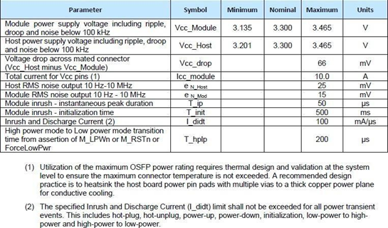
Figure 7
IX. Management Interface
Digital Diagnostic Memory Map
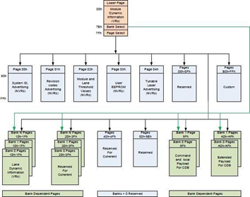
Figure 8
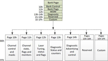
Figure 9
Multiple Applications Supported
The 800G OSFP SR8 supports 6 applications: 800GBASE-SR8,400GBASE-SR8, 200GBASE-SR8, 2x400GBASE-SR4, 4x 200GBASE-SR2,and 8x 100GBASE-SR1.
The host can select Applications by programming the AppSel value in Staged Set 0. AppSel=1 is the default Application populated in the Active Control Set at power-on or reset.
Note: that the channels of the module are independent and can be configured separately.(ie. up to eight 100GBASE- SR instances can be configured), however, it does not support different applications with different channels at the same time
The 800G OSFP SR8 supports two methods of application selection and instantiation. The first method is implemented according to CMIS, and the second method is customized, which is simpler.
First method:
The applications switching configuration sequence is as follows: read Application Descriptor Registers and select the required Appsel. Write application configuration to DPConfigLane in Stage Control Set 0, then write 1 to ApplyDPInitLane to trigger Application Instantiation. The Active Set can be read from page11h. For example, select AppDescriptor3:
Step 1: Write 0x30 in Page10h Byte145 ~ Byte152(8 bytes)—Set AppselCode3
Step 2: Write 0xFF in Page10h Byte143 — Set trigger register to run Application Instantiation.
Second method:
Set the value of Page10h Byte240. This is a private definition.
Table 8 Private Host Electrical Interface Codes
|
Code Value |
Bit Pattern |
Host Electrical Interface |
Media Interface |
|
0 |
00000000b |
100GAUI-1-S C2M |
100GBASE-SR1 |
|
1 |
00000001b |
400GAUI-8 |
400GBASE-SR8 |
|
2 |
00000010b |
200GAUI-8 |
200GBASE-SR8 |
|
3 |
00000011b |
800G S C2M |
800G-SR8 |
|
4 |
00000100b |
400GAUI-4-S C2M |
400GBASE-SR4 |
|
5 |
00000101b |
200GAUI-2-S C2M |
200GBASE-SR2 |
X. Mechanical Specifications (Unit: mm)
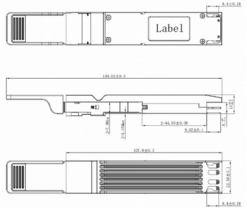
Pull tab color: Beige
Figure 10 Mechanical Dimensions
MPO-16 APC connector
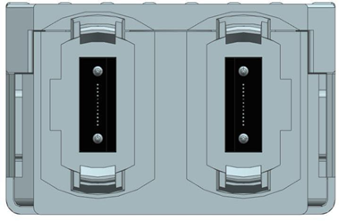
Dual MPO-12 APC connector
Figure 11 Optical Interface
Want to know about this product?
If you are interested in our products and want to know more details,please leave a message here,we will reply you as soon as we can.
 LPWWMM85-S05C
 LPWWDT11-M(L)XXC(I)

Address : East of 2F, Tianmen Optical Valley Science Park,Qiaoxiang Economic development area,Tianmen, Hubei Province.
Tel : 15012662571
Email : chris.peng@talptech.com
Skype : 15012662571