APPLICATIONS
l 800GBASE-SR8 800G Ethernet
Compliance
l QSFP-DD MSA.
l IEEE802.3db
l RoHS
Ordering information
|
Part NO. |
Bit Rate (Gbps) |
Laser (nm) |
Distance(m) |
Media |
DDMI |
Connector |
Temp(℃) |
|
ESWWMM85-S05C |
800 |
850 |
50/30 (OM4/OM3) |
multi-mode fiber |
YES |
MPO-16(APC) |
0~70 |
I. Pin Diagram
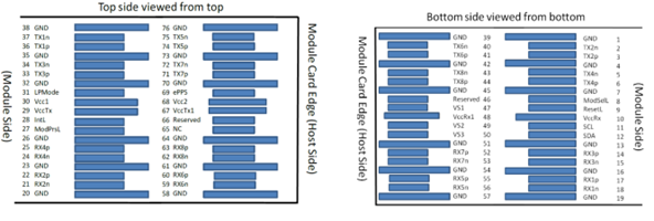
Figure 1
II. Pin Descriptions
|
Pad |
Symbol |
Description |
Ref. |
|
1 |
GND |
Ground |
|
|
2 |
Tx2n |
Transmitter Inverted Data Input |
|
|
3 |
Tx2p |
Transmitter Non-Inverted Data Input |
|
|
4 |
GND |
Ground |
|
|
5 |
Tx4n |
Transmitter Inverted Data Input |
|
|
6 |
Tx4p |
Transmitter Non-Inverted Data Input |
|
|
7 |
GND |
Ground |
|
|
8 |
ModSelL |
Module Select |
|
|
9 |
ResetL |
Module Reset |
|
|
10 |
VccRx |
+3.3V Power Supply Receiver |
|
|
11 |
SCL |
2-wire serial interface clock |
|
|
12 |
SDA |
2-wire serial interface data |
|
|
13 |
GND |
Ground |
|
|
14 |
Rx3p |
Receiver Non-Inverted Data Output |
|
|
15 |
Rx3n |
Receiver Inverted Data Output |
|
|
16 |
GND |
Ground |
|
|
17 |
Rx1p |
Receiver Non-Inverted Data Output |
|
|
Pad |
Symbol |
Description |
Ref. |
|
18 |
Rx1n |
Receiver Inverted Data Output |
|
|
19 |
GND |
Ground |
|
|
20 |
GND |
Ground |
|
|
21 |
Rx2n |
Receiver Inverted Data Output |
|
|
22 |
Rx2p |
Receiver Non-Inverted Data Output |
|
|
23 |
GND |
Ground |
|
|
24 |
Rx4n |
Receiver Inverted Data Output |
|
|
25 |
Rx4p |
Receiver Non-Inverted Data Output |
|
|
26 |
GND |
Ground |
|
|
27 |
ModPrsL |
Module Present |
|
|
28 |
IntL |
Interrupt |
|
|
29 |
VccTx |
+3.3V Power supply transmitter |
|
|
30 |
Vcc1 |
+3.3V Power supply |
|
|
31 |
LPMode |
Low Power mode; |
|
|
32 |
GND |
Ground |
|
|
33 |
Tx3p |
Transmitter Non-Inverted Data Input |
|
|
34 |
Tx3n |
Transmitter Inverted Data Input |
|
|
35 |
GND |
Ground |
|
|
36 |
Tx1p |
Transmitter Non-Inverted Data Input |
|
|
37 |
Tx1n |
Transmitter Inverted Data Input |
|
|
38 |
GND |
Ground |
|
|
39 |
GND |
Ground |
|
|
40 |
Tx6n |
Transmitter Inverted Data Input |
|
|
41 |
Tx6p |
Transmitter Non-Inverted Data Input |
|
|
42 |
GND |
Ground |
|
|
43 |
Tx8n |
Transmitter Inverted Data Input |
|
|
44 |
Tx8p |
Transmitter Non-Inverted Data Input |
|
|
45 |
GND |
Ground |
|
|
46 |
Reserved |
For future use |
|
|
47 |
VS1 |
Module Vendor Specific 1 |
|
|
48 |
VccRx1 |
3.3V Power Supply |
|
|
49 |
VS2 |
Module Vendor Specific 2 |
|
|
50 |
VS3 |
Module Vendor Specific 3 |
|
|
51 |
GND |
Ground |
|
|
52 |
Rx7p |
Receiver Non-Inverted Data Output |
|
|
53 |
Rx7n |
Receiver Inverted Data Output |
|
|
54 |
GND |
Ground |
|
|
55 |
Rx5p |
Receiver Non-Inverted Data Output |
|
|
Pad |
Symbol |
Description |
Ref. |
|
56 |
Rx5n |
Receiver Inverted Data Output |
|
|
57 |
GND |
Ground |
|
|
58 |
GND |
Ground |
|
|
59 |
Rx6n |
Receiver Inverted Data Output |
|
|
60 |
Rx6p |
Receiver Non-Inverted Data Output |
|
|
61 |
GND |
Ground |
|
|
62 |
Rx8n |
Receiver Inverted Data Output |
|
|
63 |
Rx8p |
Receiver Non-Inverted Data Output |
|
|
64 |
GND |
Ground |
|
|
65 |
NC |
No Connect |
|
|
66 |
Reserved |
For future use |
|
|
67 |
VccTx1 |
3.3V Power Supply |
|
|
68 |
Vcc2 |
3.3V Power Supply |
|
|
69 |
Reserved |
For future use |
|
|
70 |
GND |
Ground |
|
|
71 |
Tx7p |
Transmitter Non-Inverted Data Input |
|
|
72 |
Tx7n |
Transmitter Inverted Data Input |
|
|
73 |
GND |
Ground |
|
|
74 |
Tx5p |
Transmitter Non-Inverted Data Input |
|
|
75 |
Tx5n |
Transmitter Inverted Data Input |
|
|
76 |
GND |
Ground |
|
III. Absolute Maximum Ratings
|
Parameter |
Symbol |
Min. |
Typ. |
Max. |
Unit |
Ref. |
|
Storage Temperature |
TS |
-40 |
|
85 |
ºC |
|
|
Storage Ambient Humidity |
HA |
5 |
|
85 |
% |
|
|
Maximum Supply Voltage |
VCC |
-0.5 |
|
3.6 |
V |
|
|
Receiver damage Threshold,per lane |
|
5 |
|
|
dBm |
|
|
Lead Soldering Temperature/Time |
TSOLD |
|
|
260/10 |
ºC/sec |
Note1 |
|
Lead Soldering Temperature/Time |
TSOLD |
|
|
360/10 |
ºC/sec |
Note2 |
Notes:
1. Suitable for wave soldering.
2. Only for soldering by iron.
IV. Recommended Operating Conditions
|
Data Rate Spcifications |
Symbol |
Min. |
Typ. |
Max. |
Unit |
Ref. |
|
Supply Voltage |
Vcc |
3.135 |
3.3 |
3.465 |
V |
|
|
Supply Noise |
|
|
|
25 |
mVpp |
|
|
Operating Case Temperature |
Tc |
0 |
|
70 |
℃ |
|
|
Link distance on OM3 MMF |
d |
|
|
30 |
meters |
|
|
Link distance on OM4 MMF |
d |
|
|
50 |
meters |
|
V. Optical Characteristics
|
Parameter |
Symbol |
Min. |
Typ. |
Max. |
Unit |
Ref. |
||
|
Transmitter(per lane) |
||||||||
|
Channel data rate |
fDC |
106.25 |
Gb/s |
|
||||
|
Signaling rate |
FSG |
53.125 |
GBd |
PAM4 |
||||
|
Signal speed variation from nominal |
⊿fSG |
-100 |
|
+100 |
Ppm |
|
||
|
Center Wavelength |
λC |
842 |
|
868 |
nm |
|
||
|
RMS Spectral Width |
σ |
|
|
0.65 |
nm |
Note1 |
||
|
Average Launch power ,each lane |
|
-4.6 |
|
4.0 |
dBm |
|
||
|
Outer Optical Modulation Amplitude (OMAouter), each lane |
max(TECQ, TDECQ) ≤ 1.8dB |
|
-2.6 |
|
3.5 |
dBm |
|
|
|
1.8 < max (TECQ, TDECQ) ≤ 4.4dB |
-4.4 + max(TE CQ, TDECQ) |
|||||||
|
Transmitter and dispersion eye closure for PAM4, each lane |
TDECQ |
|
|
4.4 |
dB |
|
||
|
Transmitter eye closure for PAM4 (TECQ), each lane |
TECQ |
|
|
4.4 |
|
|
||
|
Transmitter power excursion, each lane |
|
|
|
2.3 |
|
|
||
|
Average Optical Output Power of Off Transmitter, each lane |
Poff |
|
|
-30 |
dBm |
|
||
|
Extinction Ratio, each lane |
ER |
2.5 |
|
|
dB |
|
||
|
Optical return loss tolerance |
|
|
|
14 |
dB |
|
||
|
Encircled flux |
|
≥86% at 19um ≤30% at 4.5um |
|
Note 2 |
||||
|
Receiver(per lane) |
||||||||
|
Damage threshold |
|
5 |
|
|
dBm |
Note 3 |
||
|
Average receive power, each lane |
|
–6.3 |
|
4.0 |
dBm |
Note 4 |
||
|
Receive power (OMAouter), each lane |
|
|
|
3.5 |
dBm |
|
||
|
Receiver reflectance |
|
|
|
-15 |
dB |
|
||
|
Receiver sensitivity(OMA outer), each lane |
TECQ ≤ 1.8dB |
|
|
|
-4.4 |
dBm |
Note 5 Figure 2 |
|
|
1.8 < TECQ ≤ 4.4dB |
-6.2+ TECQ |
|||||||
|
Receiver Loss of Signal Indicator Assert Level |
LOSA |
-15 |
|
|
dBm |
|
||
|
Receiver Loss of Signal Indicator De-assert Level |
LOSD |
|
|
-7.5 |
dBm |
|
||
|
Hysteresis |
LOSH |
0.5 |
|
5 |
dB |
|
||
|
Stressed receiver sensitivity (OMAouter), each lane |
|
|
|
-2 |
dBm |
Note 5, 6 |
||
|
Conditions of stressed receiver sensitivity test: |
Note 7 |
|||||||
|
Stressed eye closure for PAM4(SECQ), lane under test |
4.4 |
dB |
|
|||||
|
OMAouter of each aggressor lane |
3.5 |
dBm |
|
|||||
Notes:
1. RMS spectral width is the standard deviation of the spectrum
2. If measured into type A1a.2 or type A1a.3, or A1a.4, 50 um fiber, in accordance with IEC 61280-1-4.
3. The receiver shall be able to tolerate, without damage, continuous exposure to an optical input signal having this average power level on one lane. The receiver does not have to operate correctly at this input power.
4. Average receive power, each lane (min) is not the principal indicator of signal strength. A received power below this value cannot be compliant; however, a value above this does not ensure compliance.
5. For when Pre-FEC BER is 2.4 x 10⁻⁴.
6. Measured with conformance test signal at TP3 (see 167.8.14) for the BER specified in 167.1.1.
7. These test conditions are for measuring stressed receiver sensitivity. They are not characteristics of the receiver.
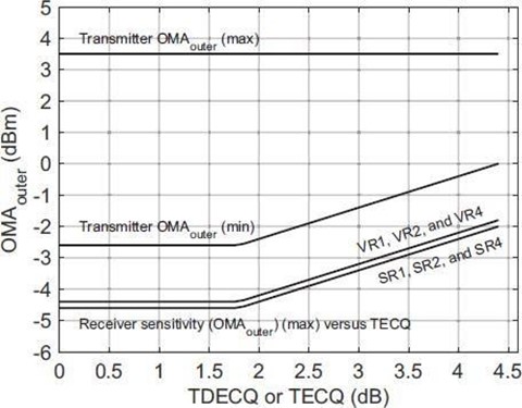
Figure 2 Receiver Sensitivity
VI. Electrical Interface Characteristics
|
Parameter |
Symbol |
Min. |
Typ. |
Max. |
Unit |
Ref. |
|
Supply Voltage |
VCC |
3.15 |
|
3.45 |
V |
|
|
Power Dissipation |
Pd |
|
|
14 |
W |
|
|
Transmitter(per Lane) |
||||||
|
Input different impedance |
Rin |
90 |
100 |
110 |
Ω |
|
|
Single ended input voltage tolerance |
VinT |
-0.4 |
|
3.3 |
V |
|
|
Differential Input Voltage Amplitude |
Vin,pp |
750 |
|
|
mV |
|
|
Receiver (per Lane) |
||||||
|
Error Bit Rate |
BER |
|
|
2.4E-4 |
|
|
|
Output different impedance |
Rout |
90 |
100 |
110 |
Ω |
|
|
Single-ended output voltage |
VoutR |
-0.4 |
|
3.3 |
V |
|
|
Differential Output Voltage Amplitude |
Vout,pp |
|
|
600/ 845 |
mV |
Short mode / Long mode |
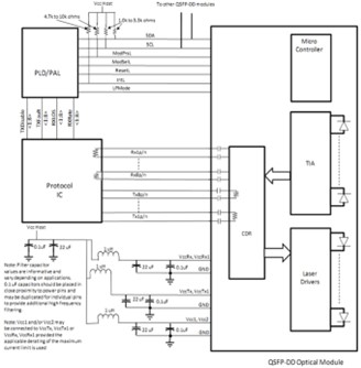
VII. Recommended Interface Circuit
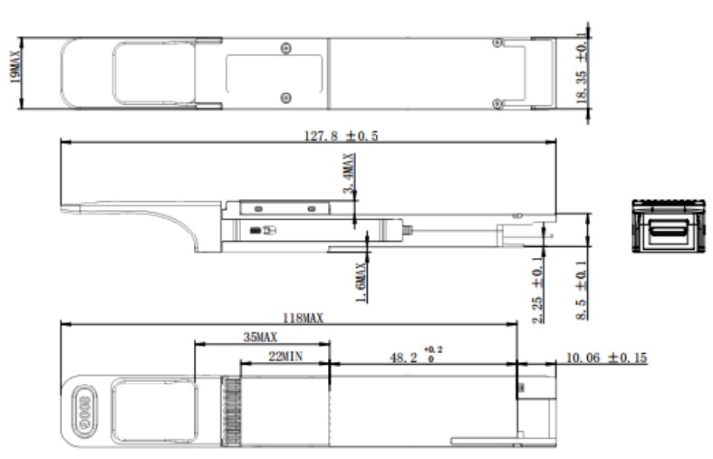
VIII.Mechanical Specifications (Unit: mm)
Want to know about this product?
If you are interested in our products and want to know more details,please leave a message here,we will reply you as soon as we can.
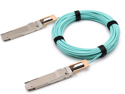
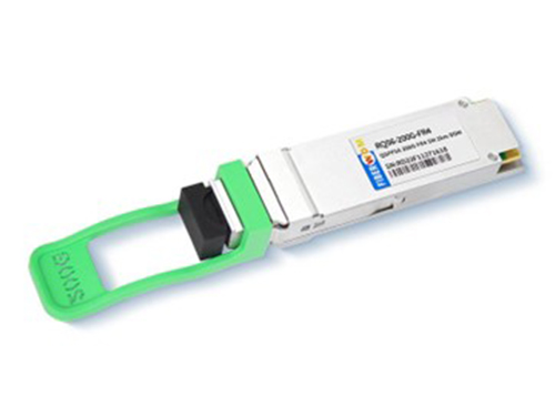
 LPXWM(H)M85-S10C
 LPWWDT11-M(L)XXC(I)

Address : East of 2F, Tianmen Optical Valley Science Park,Qiaoxiang Economic development area,Tianmen, Hubei Province.
Tel : 15012662571
Email : chris.peng@talptech.com
Skype : 15012662571