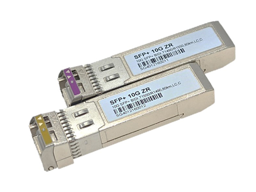
APPLICATIONS
l 10GBASE-ZR/ZW Ethernet
l 10Gb/s Fibre Channel
CPRI option 2 through 8Compliance
l SFF-8431 and SFF-8432
l SFF-8472
l ROHS
Ordering information
|
Part No. |
Bit Rate (Gbps) |
Laser (nm) |
Distance(km) |
Fiber Type |
DDMI |
Connector |
Temp |
|||||
|
ESHKLDxx1-K80C |
10.3125 |
C Lane |
80 |
SMF |
YES |
LC |
0℃~70℃ |
|||||
|
DXX1: It’s for Channel |
||||||||||||
|
Channel |
Frequency |
Center Wavelength(nm) |
Channel |
Frequency |
Center Wavelength(nm) |
|||||||
|
D17 |
191.7 |
1563.86 |
D40 |
194 |
1545.32 |
|||||||
|
D18 |
191.8 |
1563.05 |
D41 |
194.1 |
1544.53 |
|||||||
|
D19 |
191.9 |
1562.23 |
D42 |
194.2 |
1543.73 |
|||||||
|
D20 |
192 |
1561.41 |
D43 |
194.3 |
1542.94 |
|||||||
|
D21 |
192.1 |
1560.61 |
D44 |
194.4 |
1542.14 |
|||||||
|
D22 |
192.2 |
1559.79 |
D45 |
194.5 |
1541.35 |
|||||||
|
D23 |
192.3 |
1558.98 |
D46 |
194.6 |
1540.56 |
|||||||
|
D24 |
192.4 |
1558.17 |
D47 |
194.7 |
1539.77 |
|||||||
|
D25 |
192.5 |
1557.36 |
D48 |
194.8 |
1538.98 |
|||||||
|
D26 |
192.6 |
1556.55 |
D49 |
194.9 |
1538.19 |
|||||||
|
D27 |
192.7 |
1555.75 |
D50 |
195 |
1537.4 |
|||||||
|
D28 |
192.8 |
1554.94 |
D51 |
195.1 |
1536.61 |
|||||||
|
D29 |
192.9 |
1554.13 |
D52 |
195.2 |
1535.82 |
|||||||
|
D30 |
193 |
1553.33 |
D53 |
195.3 |
1535.04 |
|||||||
|
D31 |
193.1 |
1552.52 |
D54 |
195.4 |
1534.25 |
|||||||
|
D32 |
193.2 |
1551.72 |
D55 |
195.5 |
1533.47 |
|||||||
|
D33 |
193.3 |
1550.92 |
D56 |
195.6 |
1532.68 |
|||||||
|
D34 |
193.4 |
1550.12 |
D57 |
195.7 |
1531.9 |
|||||||
|
D35 |
193.5 |
1549.32 |
D58 |
195.8 |
1531.12 |
|||||||
|
D36 |
193.6 |
1548.51 |
D59 |
195.9 |
1530.33 |
|||||||
|
D37 |
193.7 |
1547.72 |
D60 |
196 |
1529.55 |
|||||||
|
D38 |
193.8 |
1546.92 |
D61 |
196.1 |
1528.77 |
|||||||
|
D39 |
193.9 |
1546.12 |
|
|
|
|||||||
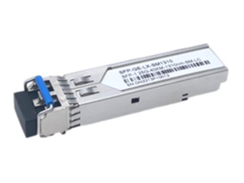
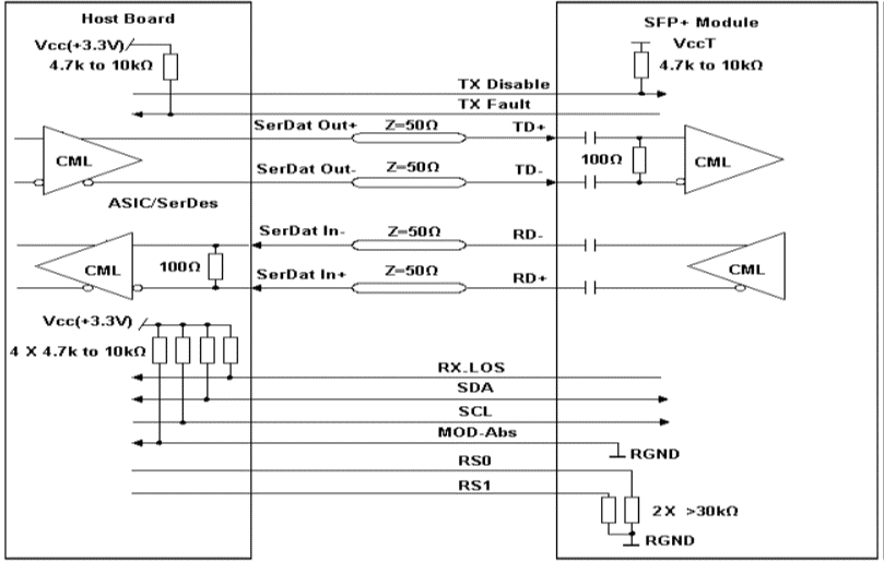
I. Pin Diagram
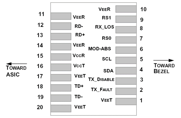
Pinout of Connector Block on Host Board
II. Pin Descriptions
|
Pin |
Symbol |
Name/Description |
Ref. |
|
1 |
VEET |
Transmitter Ground (Common with Receiver Ground) |
1 |
|
2 |
TFAULT |
Transmitter Fault. |
2 |
|
3 |
TDIS |
Transmitter Disable. Laser output disabled on high or open. |
3 |
|
4 |
MOD_DEF(2) |
Module Definition 2. Data line for Serial ID. |
4 |
|
5 |
MOD_DEF(1) |
Module Definition 1. Clock line for Serial ID. |
4 |
|
6 |
MOD_DEF(0) |
Module Definition 0. Grounded within the module. |
4 |
|
7 |
Rate Select |
No connection required |
|
|
8 |
LOS |
Loss of Signal indication. Logic “0” indicates normal operation. |
5 |
|
9 |
VEER |
Receiver Ground (Common with Transmitter Ground) |
|
|
10 |
VEER |
Receiver Ground (Common with Transmitter Ground) |
1 |
|
11 |
VEER |
Receiver Ground (Common with Transmitter Ground) |
1 |
|
12 |
RD- |
Receiver Inverted DATA out (CML). AC Coupled |
|
|
13 |
RD+ |
Receiver Non-inverted DATA out (CML). AC Coupled |
|
|
14 |
VEER |
Receiver Ground (Common with Transmitter Ground) |
1 |
|
15 |
VCCR |
Receiver Power Supply |
|
|
16 |
VCCT |
Transmitter Power Supply |
|
|
17 |
VEET |
Transmitter Ground (Common with Receiver Ground) |
1 |
|
18 |
TD+ |
Transmitter Non-Inverted DATA in. AC Coupled. |
|
|
19 |
TD- |
Transmitter Inverted DATA in. AC Coupled. |
|
|
20 |
VEET |
Transmitter Ground (Common with Receiver Ground) |
1 |
Notes:
1. Circuit ground is internally isolated from chassis ground.
2. TFAULT is an open collector/drain output, which is pulled up with a 4.7kΩ – 10kΩ resistor on the host board, but is grounded inside the SFP+ cable plug.
3. Laser output disabled on TDIS >2.0V or open, enabled on TDIS <0.8V.
4. Should be pulled up with 4.7kΩ – 10kΩ on host board to a voltage between 2.0V and 3.6V. MOD_ABS pull line low to indicate module is plugged in.
5. LOS is open collector output. Should be pulled up with 4.7kΩ – 10kΩ on host board to a voltage between 2.0V and 3.6V. Logic 0 indicates normal operation; logic 1 indicates loss of signal.
III. Absolute Maximum Ratings
|
Parameter |
Symbol |
Min |
Type |
Max |
Unit |
Ref. |
|
Maximum Supply Voltage |
Vcc |
-0.5 |
|
3.6 |
V |
|
|
Storage Temperature |
TS |
-40 |
|
85 |
℃ |
1 |
|
Case Operating Temperature |
TOP |
0 |
|
70 |
℃ |
Commercial |
|
Relative Humidity |
RH |
0 |
|
85 |
% |
2 |
Notes:
1.Limited by the fiber cable jacket, not the active ends.
2.Non-condensing.
IV. Optical Characteristics (TOP = 0°C to 70°C, VCC = 3.3 ± 5% Volts)
|
Parameter |
Symbol |
Min. |
Typ. |
Max. |
Unit |
Remark |
|
Transmitter |
||||||
|
Center Wavelength Spacing |
λ |
|
100 |
|
Ghz |
|
|
0.8 |
nm |
|
||||
|
Center Wavelength |
λC |
λ±0.1nm |
|
|
||
|
Spectral Width(-20dB) |
Pm |
|
|
1 |
nm |
|
|
Side-mode Suppression Ratio |
SMSR |
30 |
|
|
dB |
|
|
Average Output Power |
Pavg |
0 |
|
4 |
dBm |
|
|
Extinction Ratio |
ER |
9 |
|
|
dB |
|
|
Return Loss |
|
12 |
|
|
Db |
|
|
Transmitter OFF Output Power |
Poff |
|
|
-30 |
dBm |
|
|
Transmitter and Dispersion Peralty |
TDP |
|
|
3 |
dB |
|
|
Receiver |
||||||
|
Center Wavelength |
λc |
1260 |
|
1600 |
nm |
|
|
Receiver Sensitivity, Average Power |
|
|
|
-24 |
dBm |
|
|
Receiver Saturation Power |
Psat |
|
|
-8 |
dBm |
|
|
Loss of Signal Assert |
PA |
-35 |
|
|
dBm |
|
|
Loss of Signal De-assert |
PD |
|
|
-26 |
dBm |
|
|
LOS Hysteresis |
PD- PA |
0.5 |
|
|
dB |
|
V. Electrical Characteristics (TOP = 0°C to 70°C, VCC = 3.3 ± 5% Volts)
|
Parameter |
Symbol |
Min |
Type |
Max |
Unit |
Ref. |
|
Supply Voltage |
Vcc |
3.135 |
3.3 |
3.465 |
V |
|
|
Supply Current |
Icc |
|
|
480 |
mA |
|
|
Transmitter |
||||||
|
Input differential impedance |
Rin |
|
100 |
|
|
1 |
|
Differential data input swing |
Vin, pp |
200 |
|
1000 |
mV |
|
|
Transmit Disable Voltage |
VD |
2 |
|
VCC |
V |
|
|
Transmit Enable Voltage |
VEN |
Vee |
|
Vee+0.8 |
V |
|
|
Receiver |
||||||
|
Differential data output swing |
Vout, pp |
350 |
|
700 |
mV |
2 |
|
LOS Fault |
VLOS_fault |
2 |
|
Vcc |
V |
3 |
|
LOS Normal |
VLOS_norm |
Vee |
|
Vee+0.8 |
V |
3 |
|
Power Supply Noise Tolerance |
VCCT/VCCR |
Per SFF-8431 |
mVpp |
|
||
Notes:
1. Connected directly to TX data input pins.AC coupling from pins into laser driver IC.
2. Into 100Ω differential termination.
3. Loss Of Signal is LVTTL. Logic 0 indicates normal operation; logic 1 indicates no signal detected.
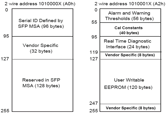
VI. Digital Diagnostic Memory Map
VII. Digital Diagnostic Monitoring Information
|
Parameter |
Unit |
Accuracy |
|
Case Temperature |
℃ |
±3 |
|
Supply Voltage |
V |
±3% |
|
Tx Bias Current |
mA |
±10% |
|
Tx Optical Power |
dB |
±3 |
|
Rx Optical Power |
dB |
±3 |
VIII.Recommended Interface Circuit
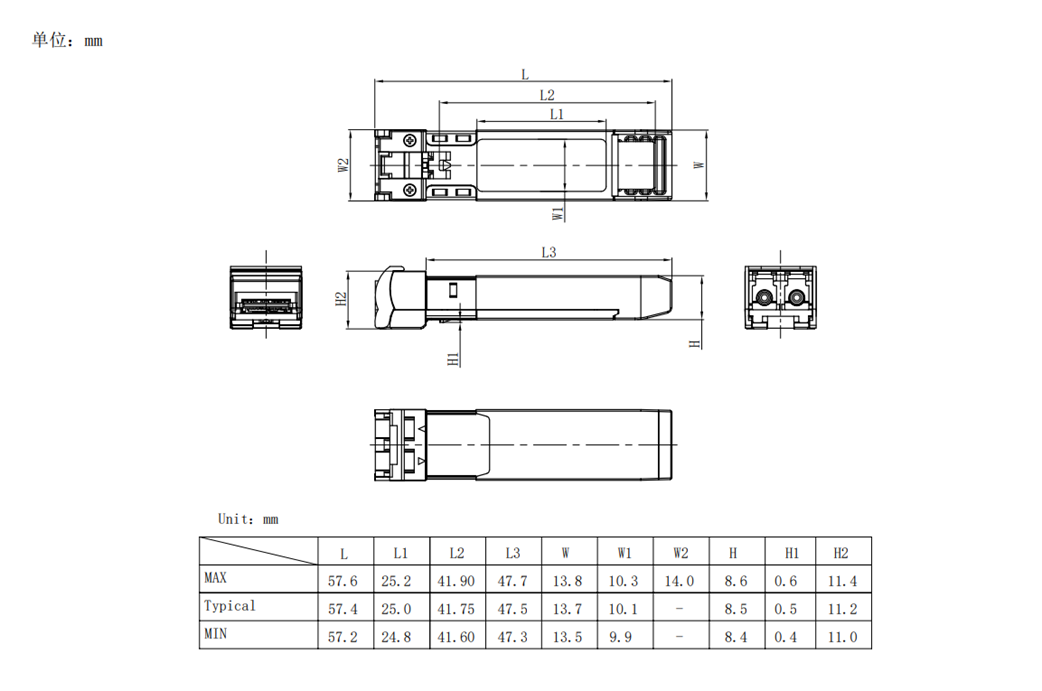
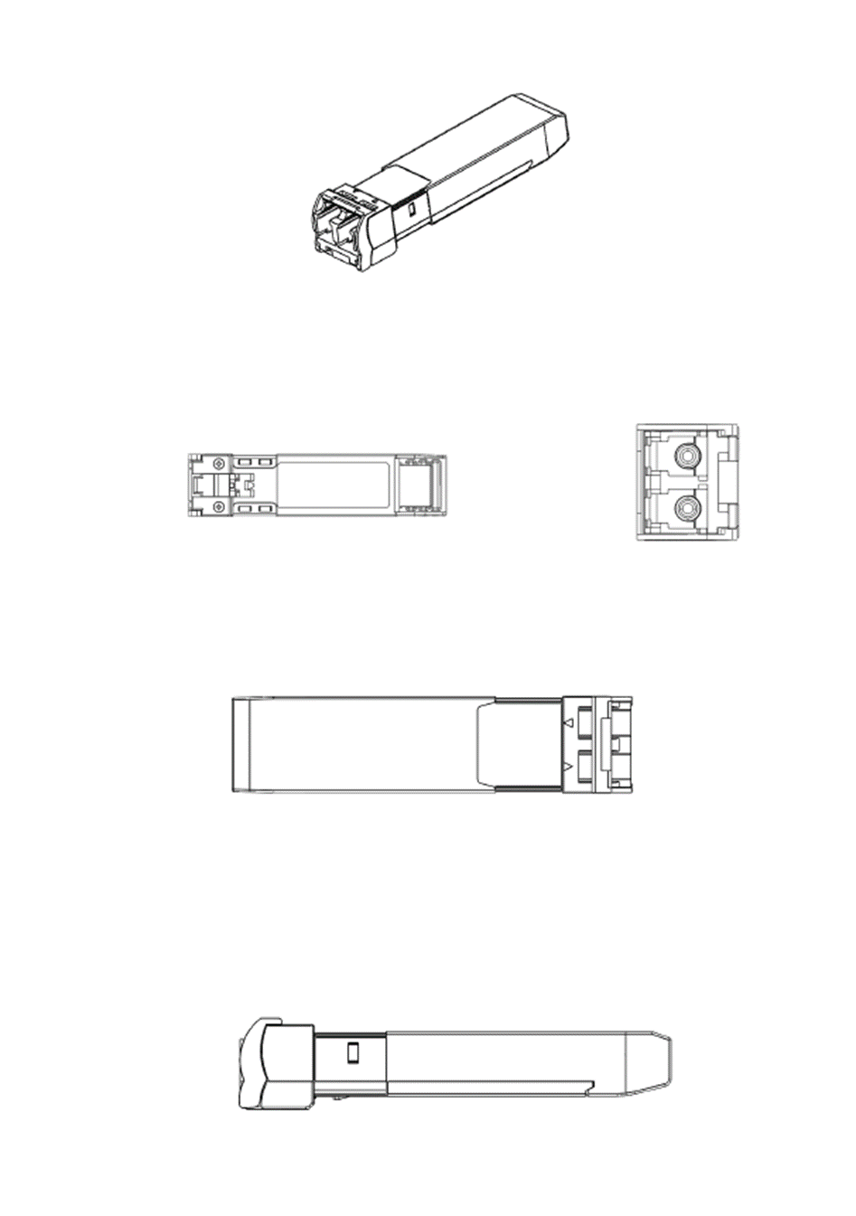
IX. Mechanical Dimensions
Want to know about this product?
If you are interested in our products and want to know more details,please leave a message here,we will reply you as soon as we can.
 LPHKLE45(54)-K80C(I)
 LPHKLB35(53)-K10C(I)
 LPHKLB23(32)-K60C(I)
 LPHKLB23(32)-K40C(I)
 LPHKLB23(32)-K40C(I)
 LPHKLB23(32)-K40C(I)
 LPHKLB23(32)-K20C(I)
 LPHKLB23(32)-K20C(I)
 LPHKLB23(32)-K20C(I)
 LPHKLB23(32)-K10C(I)

Address : East of 2F, Tianmen Optical Valley Science Park,Qiaoxiang Economic development area,Tianmen, Hubei Province.
Tel : 15012662571
Email : chris.peng@talptech.com
Skype : 15012662571