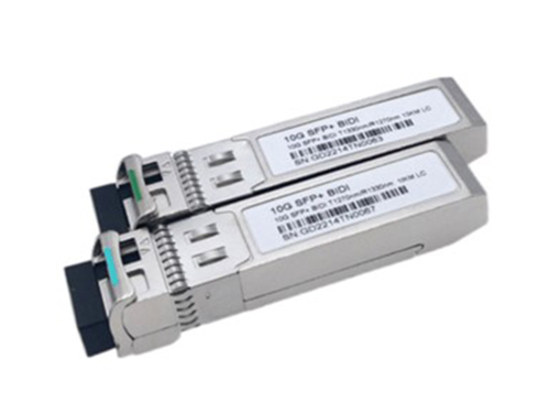
APPLICATIONS
l 10G Ethernet
l OTU2/2e
l 10G FC
l Other Optical Links
COMPLIANCE
l SFP-8431
l SFP-8432
l SFF-8472
l IEEE802.3ae
Ordering information
|
Product part NO. |
Data Rate (Gbps) |
Media |
Transmission Distance(km) |
Temperature Range(℃) |
CDR |
Power Dissipation(W) |
|
|
ESHKLE55-K80C |
10.3125 |
SMF |
80 |
0~70 |
Commercial |
Yes |
<1.5 |
|
ESHKLE55-K80I |
10.3125 |
SMF |
80 |
-40~85 |
Industrial |
Yes |
<1.8 |
I. Absolute Maximum Ratings
|
Parameter |
Symbol |
Min. |
Max. |
Unit |
|
Storage Temperature |
TS |
-40 |
+85 |
°C |
|
Maximum Supply Voltage |
VCC |
-0.5 |
3.6 |
V |
|
Operating Relative Humidity |
RH |
|
95 |
% |
II. Recommended Operating Conditions
|
Parameter |
Symbol |
Min. |
Typ. |
Max. |
Unit |
Note |
|
Case Operating Temperature |
Top |
0 |
- |
70 |
ºC |
ESHKLE55-K80C |
|
-40 |
|
85 |
ESHKLE55-K80I |
|||
|
Power Supply Voltage |
VCC |
3.13 |
3.3 |
3.47 |
V |
|
|
Data Rate |
BR |
|
10.3125 |
11.3 |
Gbps |
|
|
Transmission Distance |
TD |
|
|
80 |
km |
|
|
Coupled fiber |
Single mode fiber |
9/125um SMF |
||||
III. Electrical Characteristics (TOP = Tc, Vcc = 3.135 to 3.465 Volts)
|
Parameter |
Symbol |
Min. |
Typical |
Max. |
Unit |
Note |
|
Supply Voltage |
Vcc |
3.135 |
|
3.465 |
V |
|
|
Supply Current(Commercial) |
Icc |
|
|
450 |
mA |
|
|
Supply Current(Industrial) |
Icc |
|
|
540 |
mA |
|
|
Power Consumption(Commercial) |
P |
|
|
1.5 |
W |
|
|
Power Consumption(Industrial) |
P |
|
|
1.8 |
W |
|
|
Transmitter Section |
||||||
|
CML Inputs(Differential) |
Vin |
150 |
|
1200 |
mVpp |
1 |
|
Input Impedance(Differential) |
Zin |
85 |
100 |
115 |
ohm |
|
|
TX_DIS Disable |
|
2 |
|
Vcc+0.3 |
V |
|
|
TX_DIS Enable |
|
0 |
|
0.8 |
V |
|
|
TX_FAULT Fault |
|
2 |
|
Vcc+0.3 |
V |
|
|
TX_FAULT Normal |
|
0 |
|
0.5 |
V |
|
|
Receiver Section |
||||||
|
CML Outputs (Differential) |
Vout |
350 |
|
700 |
mVpp |
1 |
|
Output Impedance (Differential) |
Zout |
85 |
100 |
115 |
Ohm |
|
|
RX_LOS LOS |
|
2 |
|
Vcc+0.3 |
V |
2 |
|
RX_LOS Normal |
|
0 |
|
0.8 |
V |
2 |
|
MOD_DEF ( 0:2 ) VoH |
|
2.5 |
|
|
V |
With Serial ID |
|
MOD_DEF ( 0:2 ) VoL |
|
0 |
|
0.5 |
V |
With Serial ID |
Note:
1. CML logic, internally AC coupled.
2. Loss Of Signal is LVTTL. Logic 0 indicates normal operation; logic 1 indicates no signal detected.
IV. Optical Characteristics
|
Parameter |
Symbol |
Min. |
Typ. |
Max. |
Unit |
NOTE |
|
Power Budget |
|
23 |
|
|
dB |
|
|
Data Rate |
|
|
10.3125 |
11.3 |
Gbps |
|
|
Transmitter |
||||||
|
Center Wavelength |
λc |
1530 |
1550 |
1565 |
nm |
|
|
Spectral Width (-20dB) |
∆λ |
|
|
1 |
nm |
|
|
Side Mode Suppression Ratio |
SMSR |
30 |
|
|
dB |
|
|
Average Output Power |
Pout |
0 |
|
4 |
dBm |
2 |
|
Extinction Ratio |
ER |
9 |
|
|
dB |
|
|
Average Power of OFF Transmitter |
Poff |
|
|
-30 |
dBm |
|
|
Relative Intensity Noise |
RIN |
|
|
-128 |
dB/Hz |
3 |
|
Receiver |
||||||
|
Wavelength Range |
λC |
1270 |
|
1610 |
dBm |
|
|
Receiver Sensitivity |
Pmin |
|
|
-24 |
dBm |
4 |
|
Receiver Overload |
Pmax |
|
|
-8 |
dBm |
|
|
LOS De-Assert |
LOSD |
|
|
-25 |
dBm |
|
|
LOS Assert |
LOSA |
-35 |
|
|
dBm |
|
|
LOS-Hysteresis |
Phys |
0.5 |
|
|
dB |
|
Notes:
1. Corresponds to approximately 0.8 nm.
2. Output is coupled into a 9/125um SMF.
3. 12dB reflection.
4. Measured with worst ER, BER less than 1E-12 and PRBS 2^31-1 at 10.3125Gbps.
V. Digital Diagnostic Functions
|
Parameter |
Range |
Unit |
Accuracy |
Calibration |
|
Commercial Temperature |
0 to +70 |
°C |
±3°C |
Internal / External |
|
Industrial Temperature |
-40 to +85 |
°C |
±3°C |
Internal / External |
|
Voltage |
3.0 to 3.6 |
V |
±3% |
Internal / External |
|
Bias Current |
30 to 100 |
mA |
±10% |
Internal / External |
|
TX Power |
0 to +4 |
dBm |
±3dB |
Internal / External |
|
RX Power |
-23 to -6 |
dBm |
±3dB |
Internal / External |
Note:
The transceivers provide serial ID memory contents and diagnostic information about the present operating conditions by the 2-wire serial interface (SCL, SDA). The diagnostic information with internal calibration or external calibration all are implemented, including received power monitoring, transmitted power monitoring, bias current monitoring, supply voltage monitoring and temperature monitoring.
VI. Timing Characteristics
|
Parameter |
Symbol |
Min. |
Typical |
Max. |
Unit |
|
TX_Disable Assert Time |
t_off |
|
|
100 |
us |
|
TX_Disable Negate Time |
t_on |
|
|
2 |
ms |
|
Time to Initialize Include Reset of TX_FAULT |
t_int |
|
|
300 |
ms |
|
TX_FAULT from Fault to Assertion |
t_fault |
|
|
100 |
us |
|
TX_Disable Time to Start Reset |
t_reset |
10 |
|
|
us |
|
Receiver Loss of Signal Assert Time |
TA,RX_LOS |
|
|
100 |
us |
|
Receiver Loss of Signal Deassert Time |
Td,RX_LOS |
|
|
100 |
us |
|
Rate-Select Chage Time |
t_ratesel |
|
|
10 |
us |
|
Serial ID Clock Time |
t_serial-clock |
|
|
100 |
kHz |
VII. SFP Module EEPROM Information and Management
The SFP modules implement the 2-wire serial communication protocol as defined in the SFP -8472. The serial ID information of the SFP modules and Digital Diagnostic Monitor parameters can be accessed through the I2C interface at address A0h and A2h.
The memory is mapped in Table 1.
Detailed ID information (A0h) is listed in Table 2.
And the DDM specification at address A2h.
For more details of the memory map and byte definitions, please refer to the SFF-8472, “Digital Diagnostic Monitoring Interface for Optical Transceivers”. The DDM parameters have been internally calibrated.
Table 1- Digital Diagnostic Memory Map (Specific Data Field Descriptions)
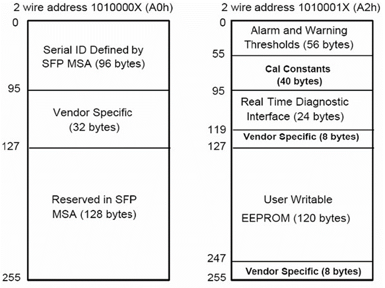
Table 2 - EEPROM Serial ID Memory Contents (A0h)
|
Data Address |
Length (Byte) |
Name of Length |
Description and Contents |
|
Base ID Fields |
|||
|
0 |
1 |
Identifier |
Type of Serial transceiver (03h=SFP) |
|
1 |
1 |
Reserved |
Extended identifier of type serial transceiver (04h) |
|
2 |
1 |
Connector |
Code of optical connector type (07=LC) |
|
3-10 |
8 |
Transceiver |
10G Base-ER |
|
11 |
1 |
Encoding |
64B/66B |
|
12 |
1 |
BR, Nominal |
Nominal baud rate, unit of 100Mbps |
|
13-14 |
2 |
Reserved |
(0000h) |
|
15 |
1 |
Length(9um) |
Link length supported for 9/125um fiber, units of 100m |
|
16 |
1 |
Length(50um) |
Link length supported for 50/125um fiber, units of 10m |
|
17 |
1 |
Length(62.5um) |
Link length supported for 62.5/125um fiber, units of 10m |
|
18 |
1 |
Length(Copper) |
Link length supported for copper, units of meters |
|
19 |
1 |
Reserved |
|
|
20-35 |
16 |
Vendor Name |
SFP vendor name: LIGHTREND |
|
36 |
1 |
Reserved |
|
|
37-39 |
3 |
Vendor OUI |
SFP transceiver vendor OUI ID |
|
40-55 |
16 |
Vendor PN |
Part Number: “LXP-H55” (ASCII) |
|
56-59 |
4 |
Vendor rev |
Revision level for part number |
|
60-62 |
3 |
Reserved |
|
|
63 |
1 |
CCID |
Least significant byte of sum of data in address 0-62 |
|
Extended ID Fields |
|||
|
64-65 |
2 |
Option |
Indicates which optical SFP signals are implemented (001Ah = LOS, TX_FAULT, TX_DISABLE all supported) |
|
66 |
1 |
BR, max |
Upper bit rate margin, units of % |
|
67 |
1 |
BR, min |
Lower bit rate margin, units of % |
|
68-83 |
16 |
Vendor SN |
Serial number (ASCII) |
|
84-91 |
8 |
Date code |
LIGHTREND’s Manufacturing date code |
|
92-94 |
3 |
Reserved |
|
|
95 |
1 |
CCEX |
Check code for the extended ID Fields (addresses 64 to 94) |
|
Vendor Specific ID Fields |
|||
|
96-127 |
32 |
Readable |
LIGHTREND specific date, read only |
|
128-255 |
128 |
Reserved |
Reserved for SFF-8079 |
Table 3 - Alarm and Warning Thresholds (A2h)
|
Data Address |
Length (Byte) |
Name of Length |
Description and Contents |
|
Base ID Fields |
|||
|
00-01 |
2 |
Temp High Alarm |
MSB at low address |
|
02-03 |
2 |
Temp Low Alarm |
MSB at low address |
|
04-05 |
2 |
Temp High Warning |
MSB at low address |
|
06-07 |
2 |
Temp Low Warning |
MSB at low address |
|
08-09 |
2 |
Voltage High Alarm |
MSB at low address |
|
10-11 |
2 |
Voltage Low Alarm |
MSB at low address |
|
12-13 |
2 |
Voltage High Warning |
MSB at low address |
|
14-15 |
2 |
Voltage Low Warning |
MSB at low address |
|
16-17 |
2 |
Bias High Alarm |
MSB at low address |
|
18-19 |
2 |
Bias Low Alarm |
MSB at low address |
|
20-21 |
2 |
Bias High Warning |
MSB at low address |
|
22-23 |
2 |
Bias Low Warning |
MSB at low address |
|
24-25 |
2 |
TX Power High Alarm |
MSB at low address |
|
26-27 |
2 |
TX Power Low Alarm |
MSB at low address |
|
28-29 |
2 |
TX Power High Warning |
MSB at low address |
|
30-31 |
2 |
TX Power Low Warning |
MSB at low address |
|
32-33 |
2 |
RX Power High Alarm |
MSB at low address |
|
34-35 |
2 |
RX Power Low Alarm |
MSB at low address |
|
36-37 |
2 |
RX Power High Warning |
MSB at low address |
|
38-39 |
2 |
RX Power Low Warning |
MSB at low address |
|
40-41 |
2 |
Optional Laser Temp High Alarm |
MSB at low address |
|
42-43 |
2 |
Optional Laser Temp Low Alarm |
MSB at low address |
|
44-45 |
2 |
Optional Laser Temp High Warning |
MSB at low address |
|
46-47 |
2 |
Optional Laser Temp Low Warning |
MSB at low address |
|
48-49 |
2 |
Optional TEC Current High Alarm |
MSB at low address |
|
50-51 |
2 |
Optional TEC Current Low Alarm |
MSB at low address |
|
52-53 |
2 |
Optional TEC Current High Warning |
MSB at low address |
|
54-55 |
3 |
Optional TEC Current Low Warning |
MSB at low address |
|
Calibration Constants for External Calibration Option |
|||
|
56-91 |
36 |
Calibration Constants for External Calibration Option |
Refer to the SFP 8472 Rev12.4 |
|
92-94 |
3 |
Reserved |
|
|
95 |
1 |
Checksum |
Byte 95 contains the low order 8 bits of the sum of bytes 0-94 |
|
Real Time Diagnostic and Control Registers |
|||
|
96-110 |
15 |
A/D Values and Status Bits |
Refer to the SFP 8472 Rev12.4 |
|
111 |
1 |
Reserved |
Reserved (was assigned to SFF-8079). |
|
Alarm and Warning Flag Bits |
|||
|
112-117 |
6 |
Optional Alarm and Warning Flag Bits |
Refer to the SFP 8472 Rev12.4 |
|
Extended Module Control/Status Bytes |
|||
|
118-119 |
2 |
Extended Module Control/Status Bytes |
Refer to the SFP 8472 Rev12.4 |
|
Optional Page Select Byte |
|||
|
120-126 |
7 |
Vendor Specific |
Vendor specific memory addresses |
|
127 |
1 |
Optional Page Select |
Defines the page number for subsequent reads and writes to locations A2h |
|
User Accessible EEPROM Locations |
|||
|
128-247 |
120 |
User EEPROM |
User writable EEPROM |
|
Vendor Specific Control Function Locations |
|||
|
248-255 |
8 |
Vendor Specific |
Vendor specific control functions |
VIII. Pin Diagram
Diagram of Host Board Connector Block Pin Numbers and Name
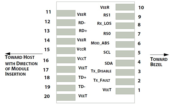
IX. Pin Descriptions
|
PIN |
Symbol |
Name/Description |
|
|
1 |
VeeT |
Module transmitter ground |
1 |
|
2 |
Tx Fault |
Module transmitter fault |
2 |
|
3 |
Tx Disable |
Transmitter Disable; Turns off transmitter laser output |
3 |
|
4 |
SDL |
2 wire serial interface data input/output (SDA) |
4 |
|
5 |
SCL |
2 wire serial interface clock input (SCL) |
4 |
|
6 |
MOD-ABS |
Module Absent, connect to VeeR or VeeT in the module |
4 |
|
7 |
RS0 |
Rate select0, optionally control SFP+ receiver. When high, input data rate >4.5Gb/ s; when low, input data rate <=4.5Gb/s |
5 |
|
8 |
LOS |
Receiver Loss of Signal Indication |
6 |
|
9 |
RS1 |
Rate select0, optionally control SFP+ transmitter. When high, input data rate >4.5Gb/s; when low, input data rate <=4.5Gb/s |
1 |
|
10 |
VeeR |
Module receiver ground |
1 |
|
11 |
VeeR |
Module receiver ground |
1 |
|
12 |
RD- |
Receiver inverted data out put |
|
|
13 |
RD+ |
Receiver non-inverted data out put |
|
|
14 |
VeeR |
Module receiver ground |
1 |
|
15 |
VccR |
Module receiver 3.3V supply |
|
|
16 |
VccT |
Module transmitter 3.3V supply |
|
|
17 |
VeeT |
Module transmitter ground |
1 |
|
18 |
TD+ |
Transmitter inverted data out put |
|
|
19 |
TD- |
Transmitter non-inverted data out put |
|
|
20 |
VeeT |
Module transmitter ground |
1 |
Note:
1. Circuit ground is internally isolated from chassis ground
2. Tx FAULT is an open collector/drain output, which should be pulled up with a 4.7k – 10k Ohms resistor on the host board if intended for use. Pull up voltage should be between 2.0V to Vcc + 0.3V.A high output indicates a transmitter fault caused by either the TX bias current or the TX output power exceeding the preset alarm thresholds. A low output indicates normal operation. In the low state, the output is pulled to <0.8V.
3. Laser output disabled on Tx DIS >2.0V or open, enabled on Tx DIS <0.8V.
4. Should be pulled up with 4.7kΩ- 10kΩ host board to a voltage between 2.0V and 3.6V. MOD_ABS pulls line low to indicate module is plugged in.
5. Internally pulled down per SFF-8431 Rev 4.1.
6. LOS is open collector output. It should be pulled up with 4.7kΩ – 10kΩ on host board to a voltage between 2.0V and 3.6V. Logic 0 indicates normal operation; logic 1 indicates loss of signal.
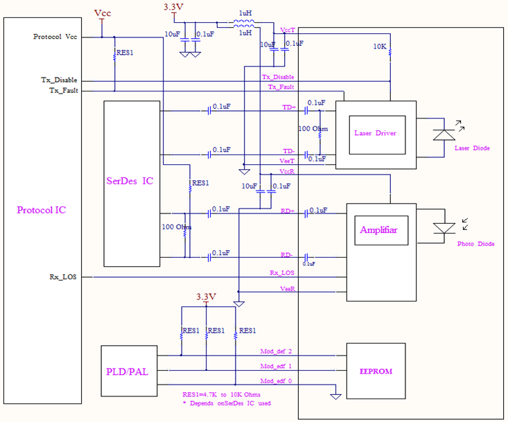
X. Recommend Circuit Schematic
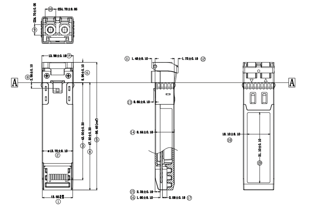
XI. Mechanical Specifications(Unit: mm)
XII. Regulatory Compliance
|
Feature |
Reference |
Performance |
|
ROHS |
BSTDG211221022108CC |
Compatible with standards |
|
EMC CE |
BSTXD211221022107EC |
Compatible with standards |
|
FCC |
BSTXD211221022118EC |
Compatible with standards |
Want to know about this product?
If you are interested in our products and want to know more details,please leave a message here,we will reply you as soon as we can.
 LPHKLE45(54)-K80C(I)
 LPHKLB35(53)-K10C(I)
 LPHKLB23(32)-K60C(I)
 LPHKLB23(32)-K40C(I)
 LPHKLB23(32)-K40C(I)
 LPHKLB23(32)-K40C(I)
 LPHKLB23(32)-K20C(I)
 LPHKLB23(32)-K20C(I)
 LPHKLB23(32)-K20C(I)
 LPHKLB23(32)-K10C(I)

Address : East of 2F, Tianmen Optical Valley Science Park,Qiaoxiang Economic development area,Tianmen, Hubei Province.
Tel : 15012662571
Email : chris.peng@talptech.com
Skype : 15012662571