
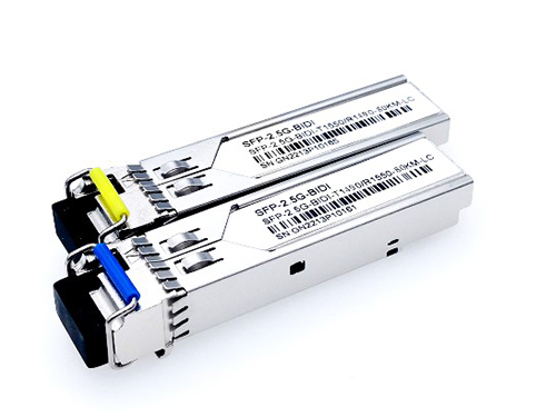
APPLICATIONS
l Fiber Channel Switch Infrastructure
l ATM Switches and Routers
l SONET / SDH Switch
l Other optical link
Compliance
l SFP MSA
l SFF-8472
l ROHS
PRODUCT SELECTIONS
|
Wavelength(nm) |
xx |
Clasp Color Code |
Wavelength (nm) |
xx |
Clasp Color Code |
|
1471 |
47 |
Gray |
1551 |
55 |
Yellow |
|
1491 |
49 |
Violet |
1571 |
57 |
Orange |
|
1511 |
51 |
Blue |
1591 |
59 |
Red |
|
1531 |
53 |
Green |
1611 |
61 |
Brown |
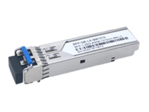
Ordering information
|
Part No. |
Bit Rate (Gbps) |
Laser (nm) |
Distance(km) |
Fiber Type |
DDMI |
Connector |
Temp |
|
ESGELCXX-Z12C |
2.488 |
1470~1610 |
120 |
SMF |
YES |
LC |
0℃~70℃ |
|
ESGELCXX-Z12E |
2.488 |
1470~1610 |
120 |
SMF |
YES |
LC |
-20℃~85℃ |
I. Pin Diagram
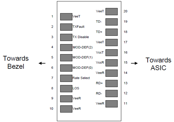
Pinout of Connector Block on Host Board
II. Pin Descriptions
|
Pin |
Symbol |
Name/Description |
Ref. |
|
1 |
VEET |
Transmitter Ground (Common with Receiver Ground) |
1 |
|
2 |
TFAULT |
Transmitter Fault. |
2 |
|
3 |
TDIS |
Transmitter Disable. Laser output disabled on high or open. |
3 |
|
4 |
MOD_DEF(2) |
Module Definition 2. Data line for Serial ID. |
4 |
|
5 |
MOD_DEF(1) |
Module Definition 1. Clock line for Serial ID. |
4 |
|
6 |
MOD_DEF(0) |
Module Definition 0. Grounded within the module. |
4 |
|
7 |
Rate Select |
No connection required |
Function not available |
|
8 |
LOS |
Loss of Signal indication. Logic “0” indicates normal operation. |
5 |
|
9 |
VEER |
Receiver Ground (Common with Transmitter Ground) |
1 |
|
10 |
VEER |
Receiver Ground (Common with Transmitter Ground) |
1 |
|
11 |
VEER |
Receiver Ground (Common with Transmitter Ground) |
1 |
|
12 |
RD- |
Receiver Inverted DATA out (CML). AC Coupled |
6 |
|
13 |
RD+ |
Receiver Non-inverted DATA out (CML). AC Coupled |
6 |
|
14 |
VEER |
Receiver Ground (Common with Transmitter Ground) |
1 |
|
15 |
VCCR |
Receiver Power Supply |
7 |
|
16 |
VCCT |
Transmitter Power Supply |
7 |
|
17 |
VEET |
Transmitter Ground (Common with Receiver Ground) |
1 |
|
18 |
TD+ |
Transmitter Non-Inverted DATA in. AC Coupled. |
|
|
19 |
TD- |
Transmitter Inverted DATA in. AC Coupled. |
|
|
20 |
VEET |
Transmitter Ground (Common with Receiver Ground) |
1 |
Notes:
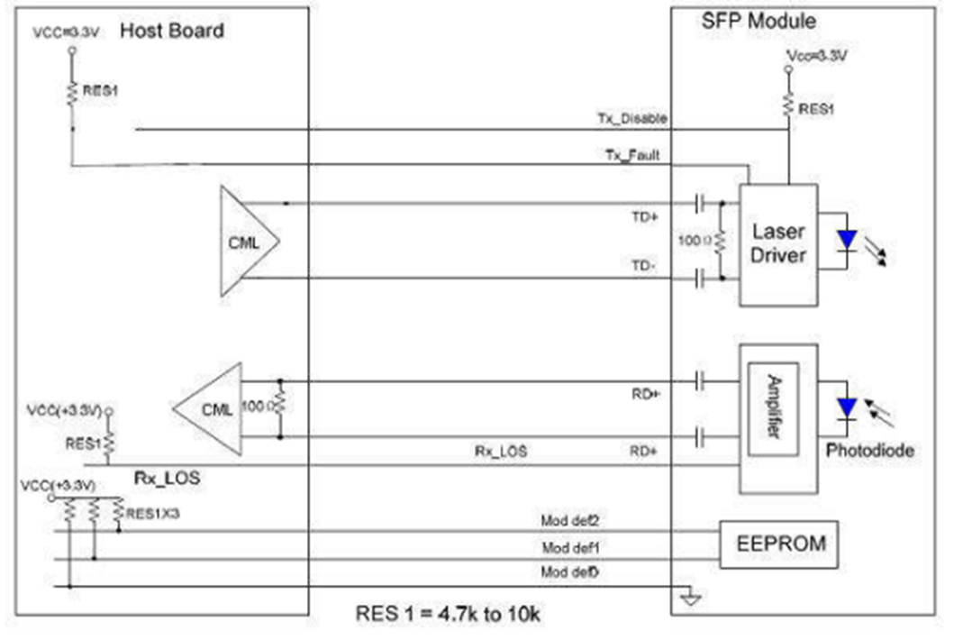
1. VeeR and VeeT may be internally connected within the SFP module.
2. TX Fault is an open collector/drain output, which should be pulled up with a 4.7K – 10KΩ
resistor on the host board. Pull up voltage between 2.0V and VccT, R+0.3V. When high, output
indicates a laser fault of some kind. Low indicates normal operation. In the low state, the output
will be pulled to < 0.8V.
3. TX disable is an input that is used to shut down the transmitter optical output. It is pulled up
within the module with a 4.7 – 10 KΩ resistor. Its states are:
Low (0 – 0.8V): Transmitter on
(>0.8, < 2.0V): Undefined
High (2.0 – 3.465V): Transmitter Disabled
Open: Transmitter Disabled
4. Mod-Def 0,1,2. These are the module definition pins. They should be pulled up with a 4.7K – 10KΩ resistor on the host board. The pull-up voltage shall be VccT or VccR
Mod-Def 0 is grounded by the module to indicate that the module is present
Mod-Def 1 is the clock line of two wire serial interface for serial ID
Mod-Def 2 is the data line of two wire serial interface for serial ID
5. VeeR and VeeT may be internally connected within the SFP module.
6. RD-/+: These are the differential receiver outputs. They are AC coupled 100Ω differential lines which should be terminated with 100Ω (differential) at the user SERDES. The AC coupling is done inside the module and is thus not required on the host board. The voltage swing on these lines will be between 400 and 2000 mV differential (200 –1000 mV single ended) when properly terminated.
7. VccR and VccT are the receiver and transmitter power supplies. They are defined as 3.3V
±5% at the SFP connector pin. Maximum supply current is 300mA. Recommended host board
power supply filtering is shown below. Inductors with DC resistance of less than 1 ohm should be used in order to maintain the required voltage at the SFP input pin with 3.3V supply voltage.
When the recommended supply-filtering network is used, hot plugging of the SFP transceiver
module will result in an inrush current of no more than 30Ma greater than the steady state value. 8. VccR and VccT may be internally connected within the SFP transceiver module.
TD-/+: These are the differential transmitter inputs. They are AC-coupled, differential lines with
100Ω differential termination inside the module. The AC coupling is done inside the module and
is thus not required on the host board. The inputs will accept differential swings of 400 – 2000mV (200 – 1000mV single-ended).
III. Absolute Maximum Ratings
|
Parameter |
Symbol |
Min |
Type |
Max |
Unit |
Ref. |
|
Maximum Supply Voltage |
Vcc |
-0.5 |
|
3.6 |
V |
|
|
Storage Temperature |
TS |
-20 |
|
85 |
℃ |
|
|
Case Operating Temperature |
TOP |
0 |
|
70 |
℃ |
Commercial |
|
-20 |
|
85 |
Extended |
|||
|
Storage Ambient Humidity |
RH |
5 |
|
95 |
% |
1 |
Notes:
1. Non-condensing.
IV. Optical Characteristics (TOP = 0°C to 70°C, VCC = 3.3 ± 5% Volts)
(CWDM DFB and APD)
|
Parameter |
Symbol |
Min. |
Typ. |
Max. |
Unit |
Remark |
|
Power Budget |
|
29 |
|
|
dB |
|
|
Transmitter |
||||||
|
Center Wavelength |
λc |
λc -6 |
λc |
λc+7.5 |
nm |
|
|
Spectral Width(-20dB) |
Pm |
|
|
1 |
nm |
|
|
Side-mode Suppression Ratio |
SMSR |
30 |
|
|
dB |
|
|
Average Output Power |
Pavg |
0 |
|
5 |
dBm |
|
|
Extinction Ratio |
ER |
8.2 |
|
|
dB |
|
|
Spectrum Bandwidth(-20dB) |
σ |
|
|
1 |
nm |
|
|
Rise/Fall Time(20%~80%) |
tr/tf |
|
|
150 |
Ps |
|
|
TX_Disable Assert Time |
t_off |
|
|
10 |
us |
|
|
Transmitter OFF Output Power |
Pout |
|
|
-45 |
dBm |
|
|
Receiver |
||||||
|
Center Wavelength |
λc |
1260 |
|
1610 |
nm |
|
|
Receiver overload |
Pmax |
-9 |
|
|
dBm |
|
|
Return Loss |
|
12 |
|
|
dB |
|
|
Receiver Sensitivity, Average Power |
|
|
|
-29 |
dBm |
1 |
|
Loss of Signal Assert |
PA |
-45 |
|
|
dBm |
|
|
Loss of Signal De-assert |
PD |
|
|
-30 |
dBm |
2 |
|
LOS Hysteresis |
PD- PA |
0.5 |
|
|
dB |
|
Notes:
1. Measured with Light source 1xx0nm, ER=8.2dB; BER =<10^-12 @PRBS=2^7-1 NRZ
2.When LOS De-asserted, the RX data+/- output is signal output.
V. Electrical Characteristics (TOP = 0°C to 70°C, VCC = 3.3 ± 5% Volts)
|
Parameter |
Symbol |
Min |
Type |
Max |
Unit |
Ref. |
|
Supply Voltage |
Vcc |
3.135 |
3.3 |
3.465 |
V |
|
|
Supply Current |
Icc |
|
|
300 |
mA |
|
|
Ambient Humidity |
HA |
5 |
|
70 |
% |
Non-condensing |
|
Transmission Distance |
|
|
|
120 |
km |
|
|
Coupled Fiber |
Single mode fiber |
9/125um G.652 |
||||
|
Transmitter |
||||||
|
Input differential impedance |
Rin |
85 |
100 |
115 |
Ohm |
1 |
|
Differential data input swing |
Vin, pp |
400 |
|
1600 |
mVpp |
2 |
|
Transmit Disable Voltage |
VD |
2 |
|
VCC+0.3 |
V |
|
|
Transmit Enable Voltage |
VEN |
0 |
|
0.8 |
V |
|
|
Receiver |
||||||
|
Differential data output swing |
Vout, pp |
400 |
|
1200 |
mV |
2 |
|
Output differential impedance |
Rout |
85 |
100 |
115 |
Ohm |
|
|
LOS Fault |
VLOS_fault |
2 |
|
Vcc+0.3 |
V |
3 |
|
LOS Normal |
VLOS_norm |
0 |
|
0.8 |
V |
3 |
|
MOD_DEF ( 0:2 ) |
VOH |
2.5 |
|
|
V |
|
|
VOL |
0 |
|
0.5 |
V |
|
|
Notes:
1. Connected directly to TX data input pins.AC coupling from pins into laser driver IC.
2. LVPECL logic, internally AC coupled.
3. Loss Of Signal is LVTTL. Logic 0 indicates normal operation; logic 1 indicates no signal detected.
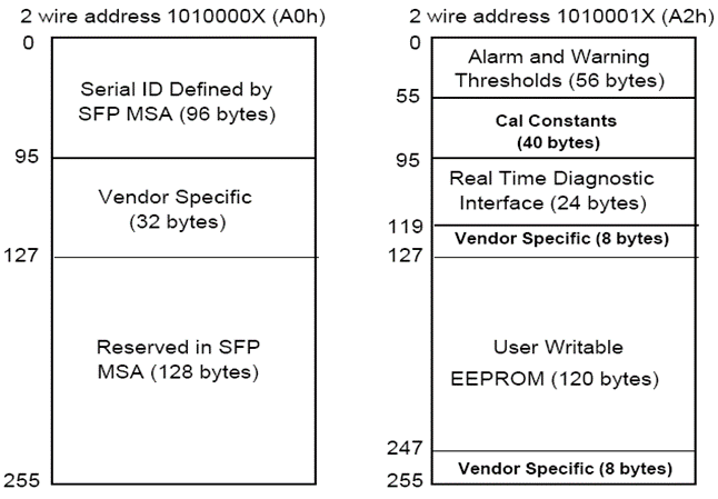
VI. Digital Diagnostic Memory Map
VII. Digital Diagnostic Monitoring Information
|
Parameter |
Unit |
Accuracy |
|
Case Temperature |
℃ |
±3 |
|
Supply Voltage |
V |
±3% |
|
Tx Bias Current |
mA |
±10% |
|
Tx Optical Power |
dB |
±3 |
|
Rx Optical Power |
dB |
±3 |
VIII.Recommended Interface Circuit
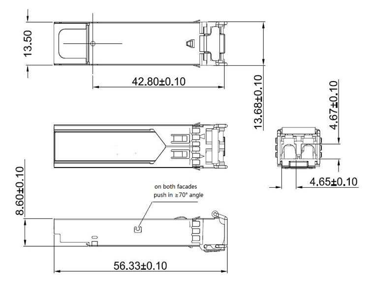
IX. Mechanical Dimensions
Want to know about this product?
If you are interested in our products and want to know more details,please leave a message here,we will reply you as soon as we can.
 LPGDLB54(B45)-K80C(I)
 LPGDLB53(B35)-K40C(I)
 LPGDLB53(B35)-K20C(I)
 LPGDLB53(B35)-K15C(I)
 LPGDLB53(B35)-K10C(I)
 LPGELDxx-Z12C
 LPGELCXX-K80C(I)
 LPGELCXX-K40C(I)
 LPGDLM85-S55C(I)
 LPGDLB55-K80C(I)

Address : East of 2F, Tianmen Optical Valley Science Park,Qiaoxiang Economic development area,Tianmen, Hubei Province.
Tel : 15012662571
Email : chris.peng@talptech.com
Skype : 15012662571