APPLICATIONS
l Switch to Switch Interface
l Fast Ethernet
l Switched Backplane Applications
l Router/Server Interface
l Other Optical Links
Compliance
l SFP MSA
l SFF-8472
l IEEE802.3z
l RoHS
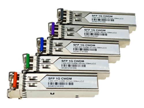
Ordering information
|
Package |
Product part NO. |
Data Rate (Gbps) |
Media |
Wavelength (nm) |
Transmission Distance(km) |
Temperature Range(℃) |
|
|
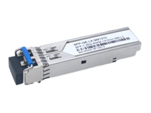
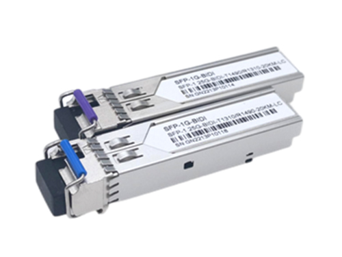
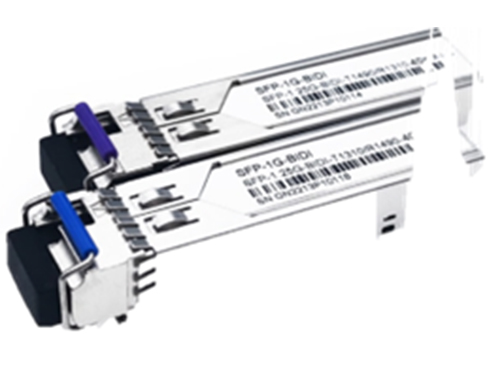
SFP |
ESGCLCxx-K90C |
1.25 |
single-mode fiber |
1xx0 |
90 |
0~70 |
Commercial |
|
SFP |
ESGCLCxx-K90E |
1.25 |
single-mode fiber |
1xx0 |
90 |
-20~85 |
Extended |
|
SFP |
ESGCLCxx-K90I |
1.25 |
single-mode fiber |
1xx0 |
90 |
-40~85 |
Industrial |
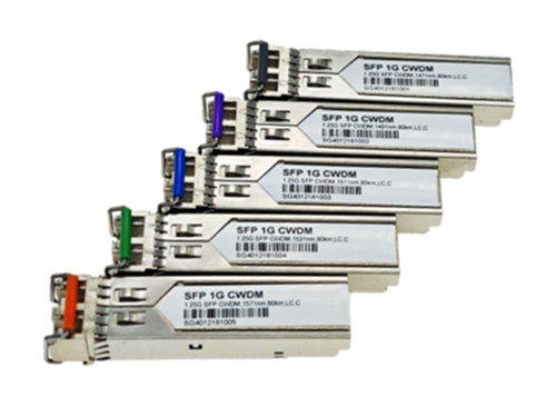
ESGCLCxx-K90C:
|
Wavelength(nm) |
xx |
Clasp Color Code |
Wavelength (nm) |
xx |
Clasp Color Code |
Wavelength (nm) |
xx |
Clasp Color Code |
|
1270 |
27 |
Gray |
1390 |
39 |
Yellow |
1510 |
51 |
Blue |
|
1290 |
29 |
Gray |
1410 |
41 |
Orange |
1530 |
53 |
Green |
|
1310 |
31 |
Gray |
1430 |
43 |
Red |
1550 |
55 |
Yellow |
|
1330 |
33 |
Purple |
1450 |
45 |
Brown |
1570 |
57 |
Orange |
|
1350 |
35 |
Blue |
1470 |
47 |
Gray |
1590 |
59 |
Red |
|
1370 |
37 |
Green |
1490 |
49 |
Purple |
1610 |
61 |
Brown |
I. Pin
Diagram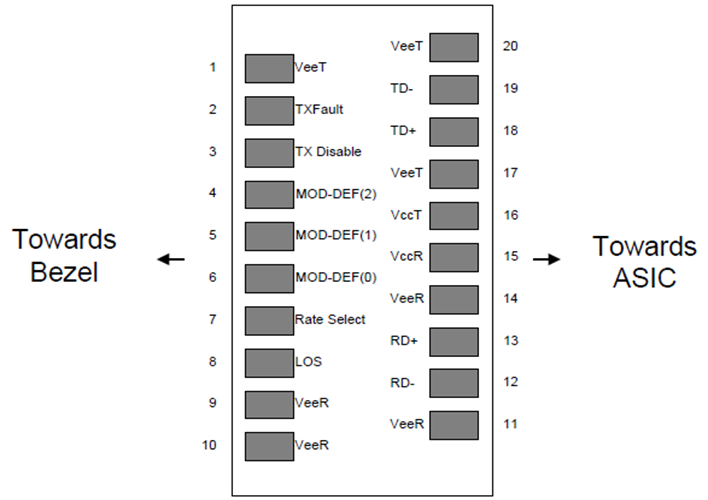
Pin out of Connector Block on Host Board
II. Pin Descriptions
|
Pin |
Symbol |
Name/Description |
Ref. |
|
1 |
VEET |
Transmitter Ground (Common with Receiver Ground) |
1 |
|
2 |
TFAULT |
Transmitter Fault.Open Drain. Logic “0” indicates normal operation. |
2 |
|
3 |
TDIS |
Transmitter Disable. Laser output disabled on high or open. |
3 |
|
4 |
MOD_DEF(2) |
Module Definition 2. Data line for Serial ID. |
4 |
|
5 |
MOD_DEF(1) |
Module Definition 1. Clock line for Serial ID. |
4 |
|
6 |
MOD_DEF(0) |
Module Definition 0. Grounded within the module. |
4 |
|
7 |
Rate Select |
No connection required. |
|
|
8 |
LOS |
Loss of Signal indication. Open Drain. Logic “0” indicates normal operation. |
5 |
|
9 |
VEER |
Receiver Ground (Common with Transmitter Ground) |
1 |
|
10 |
VEER |
Receiver Ground (Common with Transmitter Ground) |
1 |
|
11 |
VEER |
Receiver Ground (Common with Transmitter Ground) |
1 |
|
12 |
RD- |
Receiver Inverted DATA out(CML). AC Coupled |
|
|
13 |
RD+ |
Receiver Non-inverted DATA out(CML). AC Coupled |
|
|
14 |
VEER |
Receiver Ground (Common with Transmitter Ground) |
1 |
|
15 |
VCCR |
Receiver Power Supply |
|
|
16 |
VCCT |
Transmitter Power Supply |
|
|
17 |
VEET |
Transmitter Ground (Common with Receiver Ground) |
1 |
|
18 |
TD+ |
Transmitter Non-Inverted DATA in. AC Coupled. |
|
|
19 |
TD- |
Transmitter Inverted DATA in. AC Coupled. |
|
|
20 |
VEET |
Transmitter Ground (Common with Receiver Ground) |
1 |
Notes:
1. Circuit ground is internally isolated from chassis ground.
2. TX Fault is an open drain output, which should be pulled up with 4.7K – 10KΩ resistor on the host board. Pull up voltage between 2.0V to VccT/R+0.3V. When high, output indicates a laser fault of some kind. Low indicates normal operation. In the low state, the output will be pulled to < 0.8V. When sensing an improper power level in the laser driver, the SFP sets this signal high and turns off the laser. TX-FAULT can be reset with the TX-DISABLE line. The signal is in LVTTL level.
3. TX disable is an input that is used to shut down the transmitter optical output. It is pulled up within the module with 4.7K – 10KΩ resistor. Its states are: Low (0 – 0.8V): Transmitter on; (>0.8, < 2.0V): Undefined; High (2.0V to VccT/R+0.3V): Transmitter Disabled; Open: Transmitter Disabled. The TX-DISABLE signal is high (LVTTL logic “1”) to turn off the laser output. The laser will turn on when TX-DISABLE is low (LVTTL logic “0”).
4. Should be pulled up with 4.7K - 10KΩ on host board to a voltage between 2.0V to VccT/R+0.3V. MOD_DEF (0) pulls line low to indicate module is plugged in.
5. LOS (Loss of Signal) is an open collector/drain output, which should be pulled up with 4.7K – 10KΩ resistor. Pull up voltage between 2.0V to VccT/R+0.3V. When high, this output indicates the received optical power is below the worst-case receiver sensitivity (as defined by the standard in use). Low indicates normal operation. In the low state, the output will be pulled to < 0.8V.
The RX-LOS is high (LVTTL logic “1”) when there is no incoming light from the companion transceiver. This signal is normally used by the system for the diagnostic purpose. The signal is operated in LVTTL level.
III. Absolute Maximum Ratings
|
Parameter |
Symbol |
Min. |
Typ. |
Max. |
Unit |
Ref. |
|
Storage Temperature |
TS |
-40 |
|
85 |
ºC |
|
|
Storage Ambient Humidity |
HA |
5 |
|
95 |
% |
|
|
Power Supply Voltage |
VCC |
-0.5 |
|
4 |
V |
|
|
Signal Input Voltage |
|
-0.3 |
|
Vcc+0.3 |
V |
|
|
Receiver Damage Threshold |
|
+3 |
|
|
dBm |
|
|
Lead Soldering Temperature/Time |
TSOLD |
|
|
260/10 |
ºC/sec |
1 |
|
Lead Soldering Temperature/Time |
TSOLD |
|
|
360/10 |
ºC/sec |
2 |
Notes:
1. Suitable for wave soldering.
2. Only for soldering by iron.
IV. Recommended Operating Conditions
|
Parameter |
Symbol |
Min. |
Typ. |
Max. |
Unit |
Ref. |
|
Case Operating Temperature |
Tcase |
0 |
|
70 |
ºC |
ESGCLCxx-K90C |
|
-20 |
|
85 |
ESGCLCxx-K90E |
|||
|
-40 |
|
85 |
ESGCLCxx-K90I |
|||
|
Ambient Humidity |
HA |
5 |
|
70 |
% |
Non-condensing |
|
Power Supply Voltage |
VCC |
3.13 |
3.3 |
3.47 |
V |
|
|
Power Supply Current |
ICC |
|
|
300 |
mA |
|
|
Data Rate |
|
|
1250/1250 |
|
Mbps |
TX Rate/RX Rate |
|
Transmission Distance |
|
|
|
90 |
km |
|
|
Coupled Fiber |
Single mode fiber |
9/125um G.652 |
||||
V. Specification of Transmitter
|
Parameter |
Symbol |
Min. |
Typ. |
Max. |
Unit |
Ref. |
|
Average Output Power |
POUT |
0 |
|
+5 |
dBm |
|
|
Extinction Ratio |
ER |
9 |
|
|
dB |
|
|
Center Wavelength |
λC |
-6.5 |
|
+6.5 |
nm |
ESGCLCxx-K90 Note (1) |
|
Side Mode Suppression Ratio |
SMSR |
30 |
|
|
dBm |
DFB Laser |
|
Spectrum Bandwidth(-20dB) |
σ |
|
|
1 |
nm |
|
|
Transmitter OFF Output Power |
POff |
|
|
-45 |
dBm |
|
|
Jitter p-p |
tJ |
|
|
0.1 |
UI |
Note (2) |
|
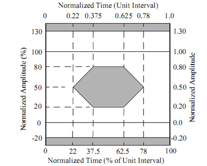
Output Eye Mask |
Compliant with IEEE802.3z (class 1 laser safety) |
|
Note (3) |
|||
Note (1): “XX” is: 27,29,31,33,35,37,39,41,43,45,47,49,51,53,55,57,59 and 61
Note (2): Measure at 2^7-1 NRZ PRBS pattern.
Note (3): Transmitter eye mask definition.
VI. Specification of Receiver
|
Parameter |
Symbol |
Min. |
Typ. |
Max. |
Unit |
Ref. |
|
Input Optical Wavelength |
λIN |
1270 |
|
1610 |
nm |
PIN/TIA |
|
Receiver Sensitivity |
PIN |
|
|
-28 |
dBm |
1 |
|
InputSaturation Power (Overload) |
PSAT |
-3 |
|
|
dBm |
|
|
Loss of Signal Assert |
PA |
-45 |
|
|
dBm |
|
|
Loss of Signal De-assert |
PD |
|
|
-33 |
dBm |
2 |
|
LOS Hysteresis |
PD-PA |
0.5 |
|
6 |
dB |
|
Notes:
1.Measured with Light source 1xx0nm, ER=9dB; BER =<10^-12 @PRBS=2^7-1 NRZ
2. When LOS De-asserted, the RX data+/- output is signal output.
VII. Digital Diagnostic Memory Map
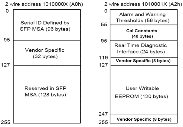
VIII.Digital Diagnostic Monitoring Information
|
Parameter |
Unit |
Accuracy |
|
Case Temperature |
℃ |
±3 |
|
Supply Voltage |
V |
±3% |
|
Tx Bias Current |
mA |
±10% |
|
Tx Optical Power |
dB |
±3 |
|
Rx Optical Power |
dB |
±3 |
IX. Electrical Interface Characteristics
|
Parameter |
Symbol |
Min. |
Typ. |
Max. |
Unit |
Ref. |
|
Transmitter |
||||||
|
Total Supply Current |
ICC |
|
|
A |
mA |
1 |
|
Transmitter Disable Input-High |
VDISH |
2 |
|
Vcc+0.3 |
V |
LVTTL |
|
Transmitter Disable Input-Low |
VDISL |
0 |
|
0.8 |
V |
|
|
Transmitter Fault Input-High |
VTxFH |
2 |
|
Vcc+0.3 |
V |
|
|
Transmitter Fault Input-Low |
VTxFL |
0 |
|
0.8 |
V |
|
|
Receiver |
||||||
|
Total Supply Current |
ICC |
|
|
B |
mA |
1 |
|
LOS Output Voltage-High |
VLOSH |
2 |
|
Vcc+0.3 |
V |
LVTTL |
|
LOS Output Voltage-Low |
VLOSL |
0 |
|
0.8 |
V |
|
Notes:
1. A (TX) + B (RX) = 300mA (Not include termination circuit)
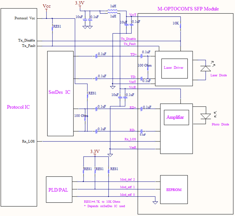
X. Recommend Circuit Schematic
XI. Mechanical Specifications (Unit: mm)
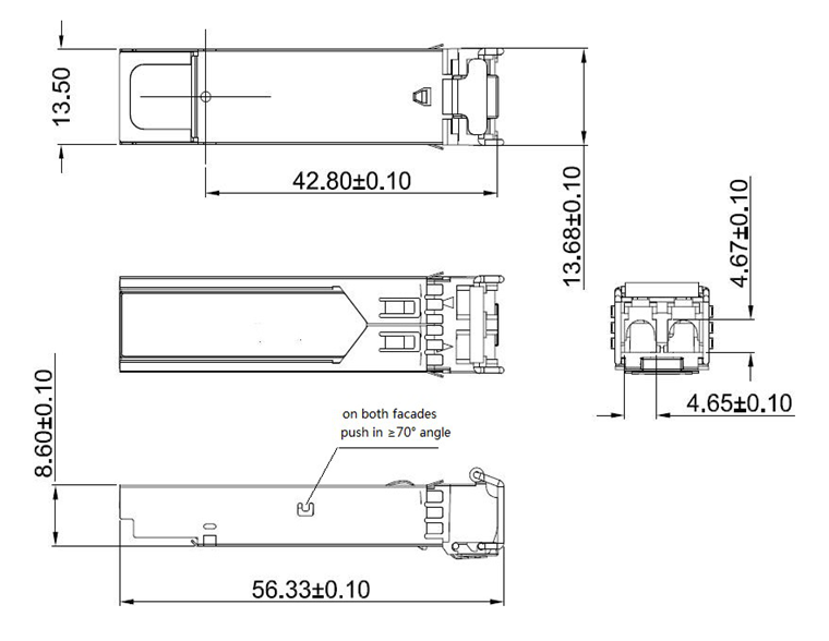
SFP wire mechanical drawing (Unit: mm)
Want to know about this product?
If you are interested in our products and want to know more details,please leave a message here,we will reply you as soon as we can.
 LPGCSB53(F35)-K20C(I)
 LPGCLF53(F35)-K03C(I)
 LPGCLB54(B45)-Z12C(I)
 LPGCLB54(B45)-K80C(I)
 LPGCLB54(B45)-K60C(I)
 LPGCLB53(F35)-K20C(I)
 LPGCLB53(B35)-K40C(I)
 LPGCLB43(F34)-K10(20)C(I)
 LPGCLB43(B34)-K40C(I)
 LPGCLCxx-Z12C

Address : East of 2F, Tianmen Optical Valley Science Park,Qiaoxiang Economic development area,Tianmen, Hubei Province.
Tel : 15012662571
Email : chris.peng@talptech.com
Skype : 15012662571